Self-assembled monolayers beyond thiols: Dithiocarbamates ...
181
Self-assembled monolayers beyond thiols: Dithiocarbamates – from pure layers to ternary assembly systems A thesis submitted in accordance with the requirement of the University of Basel for the degree of Doctor of Philosophy In the Faculty of Philosophy and Natural Science by Peter Morf from Fehraltorf (Zurich) Switzerland Villigen 2007
Transcript of Self-assembled monolayers beyond thiols: Dithiocarbamates ...
Self-assembled monolayers beyond thiols:
Dithiocarbamates – from pure layers to ternary assembly systems
A thesis submitted in accordance with the requirement of the University of Basel for the degree of
Doctor of Philosophy
In the Faculty of Philosophy and Natural Science
by
Peter Morf
from Fehraltorf (Zurich) Switzerland
Villigen 2007
Supervisor: Prof. Dr. Chr. Schönenberger Referees: Dr. T.A. Jung Dr. E. Delamarche Dean: Prof. Dr. Hans-Jakob Wirz Basel, 7. Juli 2005

Alles, was die Menschen in Bewegung setzt, muß durch ihren Kopf hindurch, aber welche Gestalt es in diesem Kopf
annimmt, hängt von den Umständen ab.
Friedrich Engels

i
Abstract Since microelectronics started to play its dominant role in the innovation of technologic and electronic instruments the reduction of the size of transistors and other functional devices was in the main focus of research and development. Therefore molecular nanotechnology and molecular electronics attracted a great deal of attention in the last years. The understanding of the fundamentals of electron transport through molecules is essential for the development and exploration of possible electronic components. Many different approaches have been introduced so far to characterise metal-molecule-metal junctions. The most reliable measurements on single molecular junctions were done on break junctions, metal gaps, which have been produced by the combination of metal microfabrication and metal electromigration as well as on the Scanning Tunneling Microscope. The molecules under investigation were almost exclusively thiol functionalised. A detailed understanding of a molecule and how it affects the transport properties of a metallic nano-gap must include the exact gap structure, the molecular backbone and the interfacial structure of the chemical/physical linker of the molecule to the metal contacts. The aim of this work was to investigate the electron transport abilities of molecules – containing dithiocarbamate (DTC) as the linker group – on the single molecular level. Therefore the chemisorption process was investigated for different aromatic and non aromatic thiol and DTC compounds by Scanning Tunneling Microscopy, X-Ray Photoelectron Spectroscopy (XPS) and Cyclic Voltammetry (CV). The obtained results were published under the title: Dithiocarbamates: Functional and Versatile Linkers for the Formation of Self-Assembled Monolayers. The most important findings presented in that publication were that the dithiocarbamates as sodium salts and also the oxidized form of dithiocarbamates the thiurams are chemisorbing in a bidentate structure on Au(111). The thiurams are decomposing at the disulfide bridge as the sodium dithiocarbamate releases the cation. Reductive desorption experiments were accomplished in a home built electrochemical set-up, which allowed for the investigation of the same samples, investigated by XPS and STM before. Comparing all these data quantitatively it was shown that the reductive desorption is a one electron transfer process.
ii
A second publication was written on the novel and very interesting surface structure of diethyldithiocarbamate: Supramolecular surface assembly of dithiocarbamates on Au(111): Chiral trimeric domains and amorphous structures. Here we report on a first time observation that chemisorbing molecules are forming trimeric complexes, which are hexagonally packed. This is the first experimental evidence of a chemisorbing supramolecular surface assembly. The next experiments were designed in order to produce STM accessible molecular surface structures i.e. islands of one molecular species placed within a matrix of another thiol compound. Therefore we investigated the formation of mixed monolayers at the solid liquid interface of a non-polar and a polar thiol species. These results will be published as: Co-assembly – concentration and mixing dependent structures: Mechanisms of molecular 2D ordering investigated by NEXAFS and STM. The most important result from this work is a detailed model, which can explain all the observed effects as there are ostwald ripening of vacancy islands, the existence of a minimal stable island size of the low dosed species and the diffusion limits of thiol adsorption. The formation of ternary assemblies comprising dithiocarbamate and thiol linked molecules within an alkanethiols self-assembled monolayer matrix made the first comparative dithiocarbamate/thiol STM study possible. A gel-assisted assembly technique enabled us to produce molecular gradient-assemblies. The combination of NEXAFS and STM lead to the identification of the molecules bound to the surface. Finally the STM data analysis lead to the first experimental evidence on the single molecular level, that dithiocarbamate is a more conductive linker than a thiolate linker. The results of these investigations were submitted under the title: Gel-assisted host/guest assembly of dithiocarbamates and thiols: Analysis of local orientation and conductivity within ternary assemblies.

iii
Table of Contents Abstract ............................................................................................................................ ii 1 Introduction ............................................................................................................... 1 2 The Fabrication of Self-Assembled Monolayers ...................................................... 5
Self-assembled monolayers (SAM) – general introduction..................................... 10 3 X-Ray Photoelectron Spectroscopy (XPS).............................................................. 15 4 Scanning Probe Microscopy (SPM) ........................................................................ 23
4.1 Scanning Tunnelling Microscopy (STM) ..................................................... 23 4.2 Atomic Force Microscopy (AFM)................................................................. 30
5 Cyclic Voltammetry ................................................................................................ 37 6 Near Edge X-Ray Absorption Fine Structure (NEXAFS) ...................................... 45
6.1 X-Ray Absorption – Theory.......................................................................... 45 6.2 X-Ray Absorption – Experimental ............................................................... 49 6.3 NEXAFS at the SIM beamline of the SLS at PSI .......................................... 51
7 Collected Publications............................................................................................. 59 8 Dithiocarbamates: functional and versatile linkers for the formation of self-
assembled monolayers. .......................................................................................... 61 8.1 Supporting Information................................................................................. 78
9 Supramolecular surface assembly of dithiocarbamates on Au(111) ..................... 83
9.1 Supporting Information................................................................................. 99 10 Co-assembly – concentration and mixing dependent binary SAMs............... 103
10.1 Supporting Information............................................................................... 132 11 Gel-assisted host/guest assembly of dithiocarbamates and thiols: .................. 135
11.1 Supporting Information............................................................................... 156 12 Publications........................................................................................................ 163 13 Curriculum Vitae ............................................................................................... 167 14 Acknowledgments ............................................................................................. 171

1
1 Introduction
Nanotechnology is one of the most interesting and progressing branch of contemporary science and especially nanobiology, nanoelectronics and nanomechanics will play an important role in the foreseeable future of scientific and technological innovation. The term “Nanotechnology” refers to technology at ultimately small scales (10-9 m) and marks the next step of technological miniaturisation. On the nanometer scale various scientific fields as chemistry, physics, material science and molecular biology meet in a natural way. From the history of science and technology we can learn that it was always fruitful when actors contributing to a certain scientific field changed to another or started an intense dialogue crossing the borders of scientific disciplines. This is exactly what is happening in the field of Nanotechnology, thus technology will be pushed forward in many different directions. The ways how very small structures can be produced may be devised into two branches. The one fabrication strategy is strongly related to microtechnology and is inspired by the downscaling of existing microtech production strategies (“top-down”) like lithography and e-beam writing. The other strategy of nanotechnological fabrication is the so-called bottom-up approach, which aims to build functional structures from molecules in thermodynamically or kinetically driven self-assembly. One of the key strengths of the self-assembly approach is that identical molecular structures can be placed in an identical atomic or molecular environment in large numbers. Due to their limited precision on the atomic scale this is virtually impossible to achieve by the use of conventional ‘top-down’, e.g. lithographic techniques. In biology, membranes, micelles etc. mostly all structural and many functional entities are self-assembled. Molecular nanotechnology involves studies about the fundamentals of various self-assembled materials. Molecular electronics, as motivated in the 1970’s from a rather theoretical point of view by Kuhn and Möbius1 and later by Aviram and Ratner,2 tries to get molecules
1 H. Kuhn and D. Möbius Angew. Chem. Int. Ed. 10 (1971) 620-637. 2 A. Aviram and M.A. Ratner Chem. Phys. Lett. 29 (1974) 277-283.

_______________________1 - Introduction________________________
2
“wired” and explore their potential use as electronic devices, logic gates or sensing entities3. The understanding of the fundamentals of electron transport through molecules is essential for the development and exploration of possible electronic components. Many different approaches have been introduced so far to characterise metal-molecule-metal junctions.4 The most reliable measurements on single molecular junctions were done on break junctions,5 metal gaps, which have been produced by the combination of metal microfabrication and metal electromigration6 as well as on the Scanning Tunneling Microscope.7,8 The molecules under investigation were almost exclusively thiol functionalized molecules. A detailed understanding of a molecule and how it affects the transport properties of a metallic nano-gap must include the exact gap structure, the molecular backbone and the interfacial structure of the chemical/physical linker of the molecule to the metal contacts. The work presented in this thesis is dedicated to a novel molecular linker group – Dithiocarbamate (DTC) – compared to the almost exclusively used thiol linker, which serves as a model system for molecular assembly on metal surfaces and for the construction of molecular electronic devices. In the first round the chemisorption and the self-assembling behaviour of DTC was investigated by Cyclic Voltammetry, X-Ray Photoelectron Spectroscopy and Scanning Tunnelling Microscopy. Chemisorption as a one electron exchange process could be proven and the electronic influence of the Au(111) surface to the DTC linking entity was determined. Later on a very interesting surface assembly structure of DEDTC, a short chain DTC, was found: the assembly in trimers. In order to investigate the electronic transport properties of the DTC molecules we studied the phase behaviour of mixed assemblies to finally be able to expose single molecules within an alkanethiol matrix to a conductive atomic force microscope tip or to a scanning tunnelling microscope tip. Here we achieved some assembly rules to finally be able to obtain small thiol islands within a decanethiol matrix. In this study 3 R. Lloyd Carroll and Christopher B. Gorman Angew. Chem. Int. Ed. 41 (2002) 4378 – 4400. 4 R. L. McCreery Chem. Mater. 16 (2004) 4477-4496. 5 J. Reichert, R. Ochs, D. Beckmann, H. B. Weber, M. Mayor, and H. v. Löhneysen Phys. Rev. Lett. 88 (2002) 176804. 6 H. S. J. van der Zant , Y-V. Kervennic , M. Poot , K. O'Neill , Z. de Groot , J. M. Thijssen , Hubert B Heersche , Nicolai Stuhr-Hansen , Thomas Bjørnholm , Daniel Vanmaekelbergh , Cornelis A van Walree , Leonardus W Jenneskens. Faraday Discuss. 131 (2006) 347-56; discussion 393-402 16512382. 7 L. A. Bumm, J. J. Arnold, T. D. Dunbar, D. L. Allara and P. S. Weiss J. Phys. Chem. B 103 (1999) 8122-8127. 8 G. V. Nazin, X. H. Qiu, and W. Ho, Science (2003) 302, 77-81.
_______________________1 - Introduction________________________
3
Near Edge X-Ray Absorption Fine Structure was used in combination with Scanning Tunnelling Microscopy. The goal of the thesis was to finally achieve ternary assembly systems, were two different molecular species are included into an alkanethiol matrix. Such a system would allow for a comparative measurement and analysis of two different molecules on the same sample. By using the gel-assisted assembly method we obtained a ternary assembly system and performed the first comparative measurement of differently linked molecules within the same layer. The DTC linked molecules exhibited a higher electron transport property than the thiol linked molecule, which highlights the possible importance of dithiocarbamate-linker for ‘molecular electronics’. This theses is organised as follows: the first chapter introduces into the fabrication of the metal and molecular films, whereas the following chapters describe the analytical tools – Scanning Probe Microscopy, X-Ray Photoelectron Spectroscopy, Cyclic Voltammetry and Near Edge X-Ray absorption Fine Structure - used to investigate the samples. The completing section consists of a compilation of four Papers collecting our major findings.

4

5
2 The Fabrication of Self-Assembled Monolayers
The first step in order to get reproducible and reliable self-assembled monolayers on gold is to produce flat and clean gold surfaces. Usually gold is evaporated on silicon wafers or on freshly cleaved mica sheets. Gold is typically evaporated by a sputtering process, by e-beam or by current heating from crucibles or wire-baskets. The evaporation of gold on silicon wafers has the advantage to exhibit a very smooth surface on large scale (~ cm). On the other hand there is the disadvantage that a chromium wetting-layer is required in order to enhance the sticking properties of gold. The existence of such a wetting layer (~ 5 nm) prohibits thorough annealing sequences of the prepared gold films; diffusion of chromium into the gold and to the gold surface has been observed. The evaporated gold on silicon-chromium surfaces can therefore not be prepared atomically flat i.e. small and round crystallites remain visible on the sample surface. From electrochemical lead deposition it is known also for such surfaces to consist mostly of Au(111) facettes (described in the cyclic voltammetry part). Raman- and IR-absorption-spectroscopy exhibit a strong signal enhancement on rough surfaces therefore gold deposited on silicon-chromium is currently used in this fields. The Raman signal is enhanced by factors up to 105 while IR-absorption shows enhancement factors of about 30-60 at such surfaces. In order to perform STM measurements on the gold films it is a mandatory requirement to use flat surfaces, otherwise the ad-layer morphology on the nanometer-scale is not detectable. In literature one can find many different recipes to produce flat Au(111) films9, fabricated by evaporation onto mica. As depicted in Figure 1 we used a BAE 250 (Balzers) evaporation vacuum chamber. The gold was evaporated by current heating of a tungsten cup. We used gold wires Ø 1mm (purity of 99.99%) from Chempur 9 Liu, Z.H. and Brown, M.D. Thin Solid Films 300 (1997) 84-94. Levelin, M.; Laakso, A.; Niemi, H.-E.-M. and Hautojärvi, P. Appl. Surf. Sci. 115 (1997) 31-38. Dishner, M.H.; Ivey, M.M.; Gorer, S.; Hemminger, J.C. and Feher, F.J. J. Vac. Sci. Technol. A 16 (1998) 3295-3300. Kobayashi, K.; Horiuchi, T. and Yamada, H. Thin Solid Films 331 (1998) 210-215. Selmantianos, N.G. and Wilson, E.G. Thin Solid Films 366 (2000) 111-116.

_________2 - The Fabrication of Self-Assembled Monolayers________
6
GmbH. The evaporation rate was monitored using a quartz crystal microbalance and the process temperature was measured next to the mica using a thermo couple. The most important parameters involved in the process to fabricate atomically flat gold films are: (I) the evaporation rate, (II) the mica temperature and (III) the annealing after the deposition.
Figure 1. The evaporation vacuum chamber Balzers BAE 250: By current heating of the gold filled tungsten cup (1) the gold starts to evaporate (2) and is condensing on a mica sheet, which is mounted on a copper plate in the heatable stage (3). A quartz crystal microbalance (4) is monitoring the evaporation rate. For stability reasons it is important to mount the microbalance on a water cooled copper tube (5) likeways to the heating contacts of the tungsten cup (6). The thermocouple next to the mica sheet reads the temperature (7) and the heating current of the mica holder can be controlled by a voltage source (8). The whole system is pumped down to the 10-9 mbar range by a turbo molecular pump (9).

_________2 - The Fabrication of Self-Assembled Monolayers________
7
Figure 2. The heatable mica holder in the evaporation chamber: The mica sheet (1) is mounted on a copper plate (2), which is fixed on insulating ceramic blocks (3). A tungsten wire is woven through holes isolated by small ceramic tubes (4). This tungsten wire can be heated by applying a voltage between the contacts (6) and ground. The temperature is read out by a thermocouple (5). The whole sample holder is mounted by screws (7). The aperture (8) is preventing the tungsten wire to be covered by gold, thus to prevent electrical short circuits.

_________2 - The Fabrication of Self-Assembled Monolayers________
8
Figure 3. The optimisation of the gold evaporation-annealing process was controlled by AFM. The here shown selection of AFM micrographs show the surface morphology depending on the some major influencing process parameters as (I) evaporation rate, (II) substrate temperature and (III) annealing temperature. Morphological features like small grain size (top left and right), molten islands (bottom left) and flat terraces (bottom right) are clarly identifie
_________2 - The Fabrication of Self-Assembled Monolayers________
9
In the literature the evaporation rate for successful Au deposition has been reported in the range of 0.5-3 Å/s. For very high rates 160 Å/s large terraces have been obtained. The second above listed parameter involves careful bake-out of the freshly cleaved mica sheet in the UHV chamber. The mica is held at elevated temperatures while the Au evaporator is started, outgassed and until the gold deposition is completed (see Figure 2). The mica sample temperatures used in this work range from 300-500 °C. The post deposition annealing can be performed in the same UHV set-up or in environmental conditions. The annealing outside the UHV chamber is usually done in an Oven or in a flame (hydrogen or pure hydrocarbons). We annealed our samples in the UHV. Atomically flat Au(111) – production using BAE 250 UHV chamber at
LMN/PSI The standard procedure has been optimised, as shown in Figure 3, in many experiments by varying the above mentioned important process parameters, namely the evaporation rate, the substrate temperature and the annealing temperature and duration. The process evaluation was always performed at residual gas pressures lower than 6104 −∗ mbar and the final gold-film thickness was adjusted to about 140nm. Our final Au(111) on mica fabrication process was the following: The mica sheet was mounted on the sample holder (Figure 2), which allowed to heat the substrate to the desired temperature. To reach 340°C substrate temperature as measured by the thermocouple, the voltage on the tungsten wire was set to 23.0 V. After 1h of de-gasing, the gold evaporation process was started only if the pressure was below 6104 −∗ mbar. At evaporation rates of 5-10 Å/s 140 nm gold were deposited on the heated mica substrate. The pressure was increasing during this process to a final pressure of 6107 −∗ mbar and the temperature was rising to 345 °C. After the gold deposition the temperature of the sample holder (thermocouple) was increased to 540°C (46-49 V, depending on the tungsten wiring) and the sample heating was kept here for a 5min post deposition anneal. Longer heating periods led to thinning of the film by sublimation. Following to this annealing process the sample was allowed to cool down in steps (500°C, 5min./ 450°C, 5min.). After switching off of the voltage source the sample equilibrated down to room temperature typically within one hour.

_________2 - The Fabrication of Self-Assembled Monolayers________
10
Self-assembled monolayers (SAM) – general introduction Early researchers realised that amphiphilic alkanethiol molecules can attach via the “metallophilic” head group to the metal and the alkyl chains subsequently form monolayer “brushes”.10 The special sulfur metal affinity is known since long time in the field of heterogenous catalysis. Early on, in 1951 Maxted investigated “The Poisioning of Metallic Catalysts” and in one chapter he is discussing the “Influence of the Molecular Size and Structure of the Poison”. Already here the concept of thiols and dithiols binding to metal surfaces and inhibiting the catalysts effectivity11 has been introduced. Figure 4 shows the structural picture drawn by Maxted. This picture is very similar to the pictures of self-assembled systems of thiols on metals, which were found 30 years later. The concept of self assembled monolyers (SAM) was found 1980 by Jacob Sagiv12. The adsorption of silanes on glass was going far beyond the usually applied Langmuir-Blodgett technique to obtain ordered thin films13. 3 years after the findings of silane SAMs Nuzzo and Allara observed the self-assembly of disulfides on gold. Due to the high stability of gold not reacting with air (oxygen) and most other chemical compounds and due to the the simple chemistry of disulfides and thiols this assembly system has evolved into the most studied organic layer system on a metal14,15,16,17. Many other chemical compounds and related substrates were found to exhibit self-assembly. A selection of such assembly pairs are shown in Table 113. Some of these systems may be more relevant in technology and other are more favorable in respect to fundamental surface science investigations. In order to perform STM experiments at high spatial resolution towards molecular electronic investigations, the substrate must be flat and not oxidised. UHV systems allow for the assembly of molecules on atomically clean substrates.
10 Emmons, H. Trans. Am. Inst. Chem. Eng. 35 (1939) 109. 11 Maxted, E.B. Advan. Catal. 3 (1951) 129. 12 Sagiv, J. J. Am. Chem. Soc. 102 (1980) 92. 13 Ulman, A. An Introduction to Ultrathin organic films Academic Press, San Diego, 1991. 14 Ulman, A. (Ed.) Thin Films, Volume 20, Organic Thin films And Surfaces, Academic Press, Boston, 1995. 15 Ulman, A. (Ed.) Thin Films, Volume 24, Self-Assembled Monolayers of Thiols, Academic Press, Boston 1998. 16 Schreiber, F. Prog. Surf. Sci. 65 (2000) 151. 17 Love, J.C.; Estroff, L.A.; Kriebel, J.K.; Nuzzo, R.G. and Whitesides, G.M. Chem. Rev. 105 (2005) 1103.

_________2 - The Fabrication of Self-Assembled Monolayers________
11
Figure 4. The special affinity of sulfur compounds i.e. thiols and disulfides to metal surfaces is well known in the field of heterogenous catalysis (Maxted 1953).
Table 1 Many different self-assembly systems.
CompoundsCarboxilic
AcidsAlco-hols
AminesAlkane-silanes
Thio-cyanates
Di-sulfides Thiols
SubstratesCu, Ag, Ni, Pd, Al2O3
Pt and Graphite
PtSiO2, SnO2,
TiO2Au Au
Au, Ag, Cu and
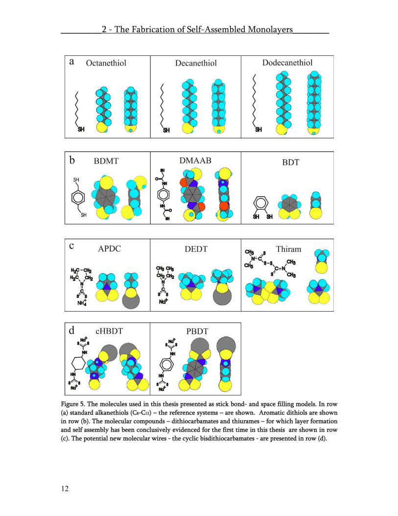
Pt On the other hand it is much more practical to take gold substrates and assemble the molecules out of solutions. In this thesis the fundamentals of chemisorbtion of dithiocarbamates on gold were explored and compared to different thiol containing compounds. In Figure 5 the set of mono-thiols, dithiols, mono-dithiocarbamates and bis-dithiocarbamates which have been investigated in this thesis are presented in a stick bond model and in a space-filling model. In this study sulfur containing compounds as shown in Figure 5. are assembled from solution to flat Au(111) surfaces.
_________2 - The Fabrication of Self-Assembled Monolayers________
12
Figure 5. The molecules used in this thesis presented as stick bond- and space filling models. In row (a) standard alkanethiols (C8-C12) – the reference systems – are shown. Aromatic dithiols are shown in row (b). The molecular compounds – dithiocarbamates and thiurames – for which layer formation and self assembly has been conclusively evidenced for the first time in this thesis are shown in row (c). The potential new molecular wires - the cyclic bisdithiocarbamates - are presented in row (d).
_________2 - The Fabrication of Self-Assembled Monolayers________
13
The molecules were dissolved in different solvents and in the case of bisdithiocarbamates the solvent was kept at high pH value to prevent decomposition under acidic influence. For all the used molecular systems we clearly observed chemisorption on gold. The alkanethiols (a) assembled as described in literature18. The dithiols (b) assembled in many different orientations and phases which could not be molecularly resolved in STM. On the other hand NEXAFS and XPS experiments performed on BDMT clearly evidenced a pre-dominant molecular orientation in the layer. For DMAAB a low degree of ordering was found in NEXAFS and STM and for BDT multi-layering was found. The small dithiocarbamates (c) APDC and DEDT could be imaged by STM and showed interesting structures, which have been compiled into a manuscript. These results are shown in the publication part titled “Self Assembly in hexagonally periodic tri-meric domains: novel self assembled monolayer systems.”. In Table 2, the special case of chirality, which does occur upon adsorption of DEDT on Au(111) is marked by red letters. Thiram (c) the only thiurame disulfide, which was tested in this series could not be molecularly resolved, but clearly chemisorbtion was observed upon decomposition of the disulfide bridge on the surface. The bisdithiocarbamates (d) clearly chemisorbed but no strong ordering was detected by NEXAFS and XPS. No molecular resolution was obtained by STM. On the other hand a very interesting meandering surface structure was found for both of these compounds. The detailed results of the chemisorption experiments is compiled into the paper “Dithiocarbamate and thiurame re-visited: self- assembled monolayers with functional and versatile end-groups”. Mixed assemblies and Gel-Assemblies, dedicated method to produce well defined host guest systems with a concentration gradient across the sample surface are also presented in the paper section.
18 Ulman, A. An Introduction to Ultrathin organic films Academic Press, San Diego, 1991. Ulman, A. (Ed.) Thin Films, Volume 20, Organic Thin films And Surfaces, Academic Press, Boston, 1995. Schreiber, F. Prog. Surf. Sci. 65 (2000) 151.

_________2 - The Fabrication of Self-Assembled Monolayers________
14
Table 2 shows different ways how a surface chirality can occur19. The DEDT on Au(111) case is indicated
by red letters.
Manifestations of Chirality Chirality of surfaceMolecularchirality point chirality Organisational Chirality
Local Chirality
GlobalChirality
(chiral motif forms on adsorption)
(domains form with molecules
in chiral arrangements) surface is surface isChiral image created
Mirror image also created
Chiral image created
Mirro image also created
==>(locally chiral
and over all racemic)
over all racemic)
no no nono no no yes yes
no no noyes yes yes yes yes
no noyes yes no yes yes yes
yes no
19 Barlow, S.M. and Raval, R. Surf. Sci. Rep. 50 (2003) 201.

15
3 X-Ray Photoelectron Spectroscopy (XPS)
X-rays were discovered by the first nobel laureate in physics, Wilhelm Conrad Röntgen (1845-1923). After observing the light emission of a fluorescence screen behind a massive obstacle exposed to the “X-Strahlen” the questions about the nature of these rays were driving the physicists to the next experiments. It was found that the X-rays were differing in their properties depending on which metal was put into the X-ray producing electron beam (in XPS Mg and Al are commonly used i.e. the Kα radiation). Max von Laue (1879-1960) proved the electromagnetic nature of the X-rays and received the Nobel Prize for “his discovery of the diffraction of X-rays by crystals”. XPS has evolved into a very powerful and commonly used surface analysis technique20,21. It allows for the chemical identification and the quantification of bound and unbound atoms on surfaces. Therefore – Kai Siegbahn (1918-) – the inventor and first promoter of this technique called it: Electron Spectroscopy for Chemical Analysis (ESCA). Kai Siegbahn was awarded by the nobel prize in physics, 1981 “for his contribution to the development of high resolution electron spectroscopy.“ The main principle of XPS is based on the idea of Albert Einstein’s photoeffect (1905). Einstein explained the discharging of metallic plates exposed to UV-radiation and/or X-rays22 by introducing a quantum effect and was awarded for the nobel prize in 1921 “for his services to theoretical physics, and especially for his discovery of the law of the photoelectric effect”. Namely, the energy of an incoming photon (quantized light) is converted into an electron, which consequently escapes from the surface.
20 Moulder, J.F.; Stickle, W.F.; Sobol, P.E. and Bomben, K.D Handbook of X-ray Photoelectron Spectroscopy Perkin-Elmer Corporation, 1992. 21 Briggs, D. and Seah, M.P. Practical Surface Analysis second edition, Volume 1, John Wiley & Sons Ltd. Chichester, 1990. 22 P. Curie and G. Sagnac: Electisation négative des rayons secondaire produits au moyen des rayons Röntgen. Compes rendus, Bd. 130. S. 1013 ff; 9. April 1900.

_____________3 - X-Ray Photoelectron Spectroscopy______________
16
Figure 6. The energy level diagram of an X-ray photoelectron spectroscopy experiment: Electrons from two atomic levels are excited by monochromatic photons (hν) and converted into free electrons. The incident photon energy, the kinetic energy of the electron and the atomic electron binding energy are directly related to each other and thus the binding energy can be obtained by determining the outgoing kinetic electron energy. The value of the binding energy allows for the identification of the atomic species and in most cases of the oxidation state.
In that time neither the quantized electronic structure of solids nor the explanation of chemical phenomena through the concept of the chemical bond was known. Quantum theory and the first experimental confirmations thereof provided deep insight into these newly emerging research fields.
_____________3 - X-Ray Photoelectron Spectroscopy______________
17
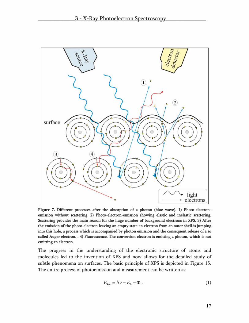
Figure 7. Different processes after the absorption of a photon (blue wave). 1) Photo-electron-emission without scattering. 2) Photo-electron-emission showing elastic and inelastic scattering. Scattering provides the main reason for the huge number of background electrons in XPS. 3) After the emission of the photo-electron leaving an empty state an electron from an outer shell is jumping into this hole, a process which is accompanied by photon emission and the consequent release of a so called Auger electron. , 4) Fluorescence. The conversion electron is emitting a photon, which is not emitting an electron.
The progress in the understanding of the electronic structure of atoms and molecules led to the invention of XPS and now allows for the detailed study of subtle phenomena on surfaces. The basic principle of XPS is depicted in Figure 15. The entire process of photoemission and measurement can be written as:
Φ−−= bkin EhE ν . (1)

_____________3 - X-Ray Photoelectron Spectroscopy______________
18
Ekin stands for the kinetic energy of the emitted electrons, hν for the incoming X-ray, Eb for the binding energy and Φ for the work function of the solid. To derive the description of the complete process, which is involved in the measurement one has to include the electron configuration i.e. the work function of the electrode. Usually the instrument is calibrated with pure metal samples in order to correct for the influence of the electrode. The electrode work function is usually a small and almost constant term, which one can neglect for most applications. The core level binding energy is dominated by the interaction with the atomic core. Therefore core level XPS allows to identify atomic species. The chemical environment has a certain influence on the electron distribution on the atom and can slightly affect the value of the core level electron binding energy. This “chemical shift” allows for the identification of different chemical species.
Figure 8. XP spectra of an octanethiol SAM on gold. Identification of the signals: many gold peaks (4s-4f), small oxygen (O1s), carbon (C1s) and sulfur (2s and 2p) peaks. For the fabrication of the thiol monolayer octanethiol was dissolved in ethanol. Solvent residues are the potential cause for the occurring oxygen species. Octanethiol is completely covering a gold surface by chemisorption and only one sulfur species is present after the layer formation i.e. no thiol is abundant anymore Note: The S2p signal consists of a characteristic double peak for 1 species.

_____________3 - X-Ray Photoelectron Spectroscopy______________
19
For the dominant coulomb contribution to the core level binding, increased charge or oxidation number generally leads to higher binding energies (the less electrons on the atom the higher the binding energy). A special feature is apparent in the higher levels of the inner shell. The spin orbit coupling causes a splitting of the energy levels i.e. the 2p level is split into the 2p1/2 and 2p3/2 state. The occupation of the states is 2 and 4, which determines the related peak intensity 2p1/2 / 2p1/2 = 2 / 4. This splitting can be detected by high resolution XPS and is shown in the inset of Figure 8. The peak splitting is not necessarily constant but equals for sulfur in the most cases 1.2 eV. Figure 3 shows the entire survey spectra of a self assembled alkanethiol monolayer. The strongest signals are indicating the gold substrate underneath the thiol layer. Carbon and sulfur are detected and a zoom into the sulfur 2p region is presented in the inset. This high resolution spectra shows that there is only one sulfur species on the surface exhibiting a sulfur 2p3/2 binding energy of 162.0 eV, which is the exact value for a thiolate layer on gold. The thiol signal is usually detected at 163.3 eV, thus the occurrence of free thiols can be excluded within the sensitivity of XPS, typically a few percent.

_____________3 - X-Ray Photoelectron Spectroscopy______________
20
Figure 9. XP spectra of diethyldithiocarbamate (DEDT) as powder and as self assembled monolayer. The powder example shows strong photoemission peaks (black) and weak auger peaks (blue). The molecule consist of C/S/N/Na (5/2/1/1) and 3 H2O per molecule. This explains the oxygen peak, but the fluorine peak (photo emission and auger) cannot be explained. The DEDT SAM shows strong gold signals, but the C, S and N peaks are clearly detectable. The Na concentration in contrary remained below detection limit, which proofs the chemisorption of the DEDT on gold.
Figure 9 presents the difference of a powder and a SAM spectrum. In the powder spectrum all the species give a reasonably high X-ray photoelectron peak and some auger peaks are identified. The commercially available diethyldithiocarbamate contains 3 molecules of crystalline water, which is the reason for the strong oxygen signal. A surprising feature is the detection of a fluorine signal in the DEDT powder

_____________3 - X-Ray Photoelectron Spectroscopy______________
21
where no straightforward explanation can be found. XPS measurements on powder samples suffer from a systematic problem: the charging of the insulating powder. If a sample is charged the electrons escaping from the surface are not anymore fulfilling the energy conservation law (equation 1) because the electron does not start from 0 potential. To compensate this effect sample internal references are used to perform differential measurements. In our study we used nitrogen as an internal reference to compare DEDT and Thiram powder spectra (N1s = 400.0 eV). The second spectra of Figure 9 shows the XP spectra of DEDT assembled on Au(111). This spectrum shows similar features like the thiol spectrum shown in Figure 8. i.e. huge gold 4 peaks and small peaks of the monolayer atoms. In the Na region no significant amount of Na is detectable, as Na has one of the highest observed X-ray photoemission cross sections (Na1s/C1s/S2p: 8.52/1.00/1.58). In order to obtain a representative and quantitative surface analysis the measured signal must be cross-section-corrected, which is usually done by the analysis software. To get a comparative quantification of two different measurements one has to normalise the signals. To compare the amount of bound sulfur on the gold surface it is reasonable to normalise the sulfur signal by the gold 4f signal. This normalisation is very reliable because the two species are abundant in close proximity on the studied samples. Therefore the electrons coming from the gold and the ones from the sulfur are not scattered by atoms between them.
Table 3. XPS Binding energies of the SAM sulfur species.
XPS-S2P Signal
CompoundBinding energy S1
[eV]Binding energy S2
[eV]RatioS1:S2
Octanethiol on gold 162.0(2)Decanethiol on gold 161.7(2)BDMT on gold 161.9(2) 163.2(2) 1:1.3Thiram bulk 161.6(2)a) 163.6(2)a) 1:1.1Thiram on gold 161.6(2)APDC on gold 161.8(2)DEDT bulk 161.6(2)a)
DEDT on gold 161.6(2)cHBDT bulk 161.9(2)b)
cHBDT on gold 161.0(2) 162.0(2) 1:1.2PBDT bulk 161.7(2)b)
PBDT on gold 161.0(2) 162.0(2) 1:3.4 a). setting N to 400eV b). setting C to 285eV and Na to 1072eV

_____________3 - X-Ray Photoelectron Spectroscopy______________
22
The qualitative analysis of self-assembled monolayers with different molecular composition as they have been studied in this thesis are shown in Table 3. The monothiols show one signal at 162 eV. The dithiol BDMT shows an additional signal of the freestanding thiol at 163 eV. The SAM forming dithiocarbamate compounds DEDT, APDC and Thiram, as they are here introduced as a new SAM forming system, show one sulfur species at roughly 162 eV. The bisdithiocarbamates exhibit an additional signal at 161 eV which originates from the thio-Na complex. The detailed discussion of these XPS results is compiled into the publication “Dithiocarbamate and Thiurame re-visited: Functional and versatile End-Groups for the formation of Self Assembled Monolayers with novel properties”, which also discusses the sulfur concentrations abundant at the surface as shown in Table 4. with special consideration of the reductive desorption experiments on these layers.
Table 4. Relative sulfur content in different SAMs.
XPS - Sulfur contents
CompoundSbound/Au ratio
S-Contentrel. to OT
error
Octanetiol 0.0409 1.00 0.12Decanetiol 0.0441 1.08 0.12BDMT 0.0470 1.15 0.06
BDT 0.0780 1.91single exp.
DEDT 0.0724 1.69 0.07APDC 0.0958 2.11 0.11Thiram 0.0966 2.36 0.20cHBDT 0.0738 1.80 0.21PBDT 0.0992 2.42 0.16
The most interesting result of the quantitative surface analysis is the much higher sulfur content in the dithicarbamate layers. Some of these results are thoroughly discussed in the manuscript “Self Assembly in hexagonally periodic tri-meric domains: novel self assembled monolayer systems.”

23
4 Scanning Probe Microscopy (SPM) The invention of scanning tunnelling microscopy (STM) by G. Binnig (1947-) and H. Rohrer (1933-) was honoured by the nobel prize23 for “their design of the scanning tunnelling microscope”. This new instrumental set-up led to a fast development of many different local probe techniques. Atomic force microscopy (AFM), lateral force microscopy (LFM), magnetic force microscopy (MFM), electrochemical STM (ECSTM), chemical force microscopy (CFM) and scanning near field optic microscopy (SNOM) are some of the whole zoo of scanning probe methods, which have been introduced since the first presentation and demonstration of STM. The first remarkable demonstration of atomic real space resolution was presented by Binning, Rohrer, Gerber and Weibel in 198324. The outstanding problem of the nature of the 7×7 reconstruction of Si(111) surfaces was solved by STM. This was the breakthrough, which was followed by instrumental improvements and a tremendous wide range of emerging experimental possibilities. Metals, metals on metals, molecules on metals and many different ad-layer-systems on diverse substrate were investigated in atomic and molecular detail25.
4.1 Scanning Tunnelling Microscopy (STM) As shown in Figure 10 the scanning tunnelling microscope (STM) is based on the combination of a fast feedback loop and a local sensitive probe. On one hand the tunnelling current between a sharp tip and a conductive sample surface is depending on the very local structure of the sample. On the other hand, the electronic feedback coupled to a piezo-crystal-tube makes a precise and fast positioning system. 23 Binnig, G. and Rohrer, H. Reviews of Modern Physics 59 (1987) 615. 24 Binnig, G.; Rohrer, H.; Gerber, Ch. and Weibel, E. Phys. Rev. Lett. 50 (1983) 120. 25 Güntherodt, H.-J. and Wiesendanger, R. (Eds.) Scanning Tunneling Microscopy I , 2nd edition, Springer Series in Surface Science Nr. 20. Springer-Verlag, Berlin, 1992. Wiesendanger, R. and Güntherodt, H.-J. (Eds.) Scanning Tunneling Microscopy II , Springer Series in Surface Science Nr. 28. Springer-Verlag, Berlin, 1992. Wiesendanger, R. and Güntherodt, H.-J. (Eds.) Scanning Tunneling Microscopy III , 2nd edtition, Springer Series in Surface Science Nr. 29. Springer-Verlag, Berlin, 1996.

________________4 - Scanning Probe Microscopy_________________
24
For STM investigations in ambient conditions we use a Veeco ‘Multimode’ microscope and a Veeco ‘Nanoscope III’ feedback controller, which is upgraded with a low current amplifier allowing for reasonable time constants of the feedback at tunnelling currents of 1 pA. This system is commercially available and is produced by Veeco (www.veeco.com). The Multimode microscope was positioned on a heavy brass plate (approx. 5 kg), which is suspended at the ceiling using elastic ropes. This simple anti-vibration system led to a very efficient noise reduction. The microscope tips were mechanically sharpend Pt/Ir (80/20) wire (0.25 mm diam.) sold by Eurotitan (www.eurotitan.co.uk, PTIR-WR-003-004). Pt/Ir is a non-oxidising material with an accurate hardness to be cut easily with a small wire cutter. While cutting the wire the wire cutter is to be pulled such that the wire is rather torn than cut for the final part. Such tips are cheap and are commonly used in the multimode set-up for investigations in ambient conditions in particular on self assembled thiol (C8, C10 and C12) monolayers on gold. Molecular resolution on standard thiol SAMs was routinely achieved using self-cut tips as described above. Some self-assembled systems were additionally investigated by using an UHV-AFM/STM distributed and produced by Omicron (www.omicron.de). For these experiments electrochemically etched tungsten tips were used as they are provided by Omicron.

________________4 - Scanning Probe Microscopy_________________
25
Figure 10. The scanning tunnelling microscope (STM) consists of two different but ideally combined features. The ideally sharp point probe, a metallic tip (1) is scanned across the sample surface (3) by using a piezo-crystal (2) based 3D scanner. While x and y are driven by the scanning software, the z-coordinate of the scanner is controlled by fast feed-back electronics (4) such that the tunnelling current is kept constant.
________________4 - Scanning Probe Microscopy_________________
26
4.1.1 STM on self assembled monolayers STM has been successfully used to investigate many molecular surface systems. In the first years (until 1990) molecular resolution could not be obtained but as time moved by astonishing details have been imaged. In the field of self assembled monolayers i.e. thiols on Au(111) STM was used for the first time by Widrig et al.26 and Häussling et al27 respectively. While Widrig measured on a pure octadecanethiolate SAM obtaining molecular resolution and finding molecule-molecule distances of 0.50±0.02 nm. These authors had been using astonishing scan parameters, i.e. 200mV bias voltage and 1-10 nA tunnelling current i.e. 0.02-0.2 GΩ tunnelling restistance, Häussling et al. tested the adsorption of biomolecules on a preformed SAM and they found additional small vacancy islands (“holes”) in the molecular ad-layer. In the following years the nature of the “holes” usually referred to as etch-pits was resolved28. After these first successful images of thiolate monolayers have been obtained, many fundamental processes of SAM formation as well as SAM layer structures structures were investigated by STM. Subject of these experiments were the domain structure and the evolution of the layer structure upon thermal annealing and upon changing the assembly parameters29, the thermal stability30, the “tip etching” of SAMs31, the superstructures32, the huge variety of low coverage phases33, the liquid phases34, the detailed mechanism of vacancy island formation35 and the electrical layer characteristics36.
26 Widrig, C.A.; Alves, C.A. and Porter, M.D. J. Am. Chem. Soc. 113 (1991) 2805. 27 Häussling, L.; Michel, B.; Ringsdorf, H. and Rohrer, H. Angew. Chem. Int. Ed. Engl. 30 (1991) 569. 28 Schönenberger, C.; Sondag-Huethorst, J.A.M.; Jorritsma, J. and Fokkink, L.G.J. Langmuir 10 (1994) 611. 29 Schönenberger, C.; Jorritsma, J.; Sondag-Huethorst, J.A.M. and Fokkink, L.G.J. J. Phys. Chem. 99 (1995) 3259. 30 E, Delamarche.; Michel, B.; Kang, H. and Gerber, Ch. Langmuir 10 (1994) 4103. Bucher, J.-P.; Santesson, L. and Kern, K. Langmuir 10 (1994) 979. 31 Kim, Y.-T. and Bard, A. Langmuir 8 (1992) 1096. 32 Poirier, G.E. and Tarlov, M.J. Langmuir 10 (1994) 2854. Noh, J. and Hara, M. lanmuir 19 (2002) 1953. Lüssem, B.; Müller-Meskamp, L. Karthäuser, S. and Waser, R. Langmuir 21 (2005) 5256. 33 Yamada, R.; Wano, H. and Uosaki, K. Langmuir 16 (2000) 5523. Xiao, X.; Wang, B.; Zhang, Chun.; Yang, Z. and Loy, M.M.T. Surface Science 472 (2001) 41. Noh, J. and Hara, M. Langmuir 17 (2001) 7280. Porier, G.E.; Fitts, W.P. and White, J.M. Langmuir 17 (2001) 1176. Fitts, W.P.; White, J.M. and Poirier, G.E. Langmuir 18 (2002) 1561. Qian, Y.; Guohua, Y.; Jingjiang, Y.; Jung, T.A and Liu, G.-Y. Langmuir 19 (2003) 6056. 34 Poirier, G.E.; Tarlov, M.J. and Rushmeier, H.E. Langmuir 10 (1994) 3383. 35 Poirier, G.E. Langmuir 13 (1997) 2019. 36 Kobayashi, K.; Horiuchi, T.; Yamada, H. and Matsushige, K. Thin Solid Films 331 (1998) 210. Labonté, A.P.; Tripp, S.L.; Reifenberger, R. and Wei A. J. Phys. Chem. B 106 (2002) 8721.

________________4 - Scanning Probe Microscopy_________________
27
After these detailed and profound studies on the structural properties of alkanethiol SAMs on gold other questions came into focus of SPM experiments. Is the self-assembly approach suitable to produce ordered mixed layers consisting of different molecular compounds? How are they packed or structured? Are such systems useful as model systems in molecular electronics? Can the desired mono-molecular experiment in molecular electronics be established by a SPM-SAM approach? As discussed in the earlier chapters of this thesis there are different ways to produce mixed monolayers systems. Molecules with potentially interesting properties, e.g. molecular ‘wires’ or ‘tweezers’ (mostly conjugated aromatic molecules) are inserted into a preformed alkanethiols monolayer forming a “host/guest”- system37. Weiss et. al. introduced a new modulation technique to probe single molecules and to differentiate between the electronic conductivity of the molecular backbone and the electronic conductivity of the contact between the chemical linker and the substrate38. Others were using conventional STM and found structural effects on electrical conduction39, effects of packing and order40, redox state dependence41, lateral island conduction42 and conductance switching43. These results are promising but not strongly reliable because quite often they remain difficult to reproduce44. The simple model of a STM tunnelling experiment on a molecular monolayer is depicted in Figure 11. Here one can see the influence of the bias potential on the probability of a resonant tunnelling situation. If the potential rises on one or the other electrode (shift of μS and μT up or down) then electrons can be transported by resonant tunnelling through the HOMO molecular state. Such a situation is symmetric and therefore would result in symmetric IV-curve.
37 Cygan,M.T.; Dunbar, T.D.; Arnold, J.J.; Bumm, L.A.; Shedlock, N.F. Burgin, T.P.; Jones II, L.; Allara, D.L.; Tour, J.M. and Weiss, P.S. J. Am. Chem. Soc. 120 (1998) 2721. 38 Chapter in “Molecular Electronics: Science and Technology” Aviram, A. and Ratner, M. (Eds.), Annals of the New York Academy of Science, Volume 852, The New York Academy of Science, 1998. 39 Ishida, T.; Mizutani, W.; Nami, Choi.; Akiba, U.; Fujihira, M. and Tokumoto, H. J. Phys. Chem. B 104 (2004) 11680. Wakamatsu, S.; Akiba, U. and Fujihira M. Colloids and Surfaces 198-200 (2002) 785. 40 Dholakia, G.R.; Wendy, Fan.; Koehne, J.; Han, J. and Meyyappan Phys. Rev. B 69 (2004) 153402. 41 Haiss, W.; van Zalinge, H.; Higgins, S.J.; Bethell, D.; Höbenreich, H. Schiffrin, D.J. and Nichols, R.J. J. Am. Chem. Soc. 125 (2003) 15294. 42 Ishida, T.; Mizutani, W.; Akiba, U.; Umemura, K.; Inoue, A.; Choi, N.; Fujihira, M. and Tokumoto, H. J. Phys. Chem. B 103 (1999) 1686. 43 Donhauser, Z.J.; Mantooth, B.A.; Kelly, K.F.; Bumm, L.A.; Monnell, J.D.; Stapleton, J.J.; Price Jr., D.W.; Rawlett, A.M.; Allara, D.L.; Tour, J.M. and Weiss, P.S. Science 292 (2001) 2303. Ramanchandran, G.K.; Hopson, T.J.; Rawlett, A.M.; Nagahara, L.A.; Primak, A. and Lindsay, S.M. Science 300 (2003) 13. 44 Rampi, M.A. and Whitesides, G.M. Chemical Physics 281 (2002) 373.
________________4 - Scanning Probe Microscopy_________________
28
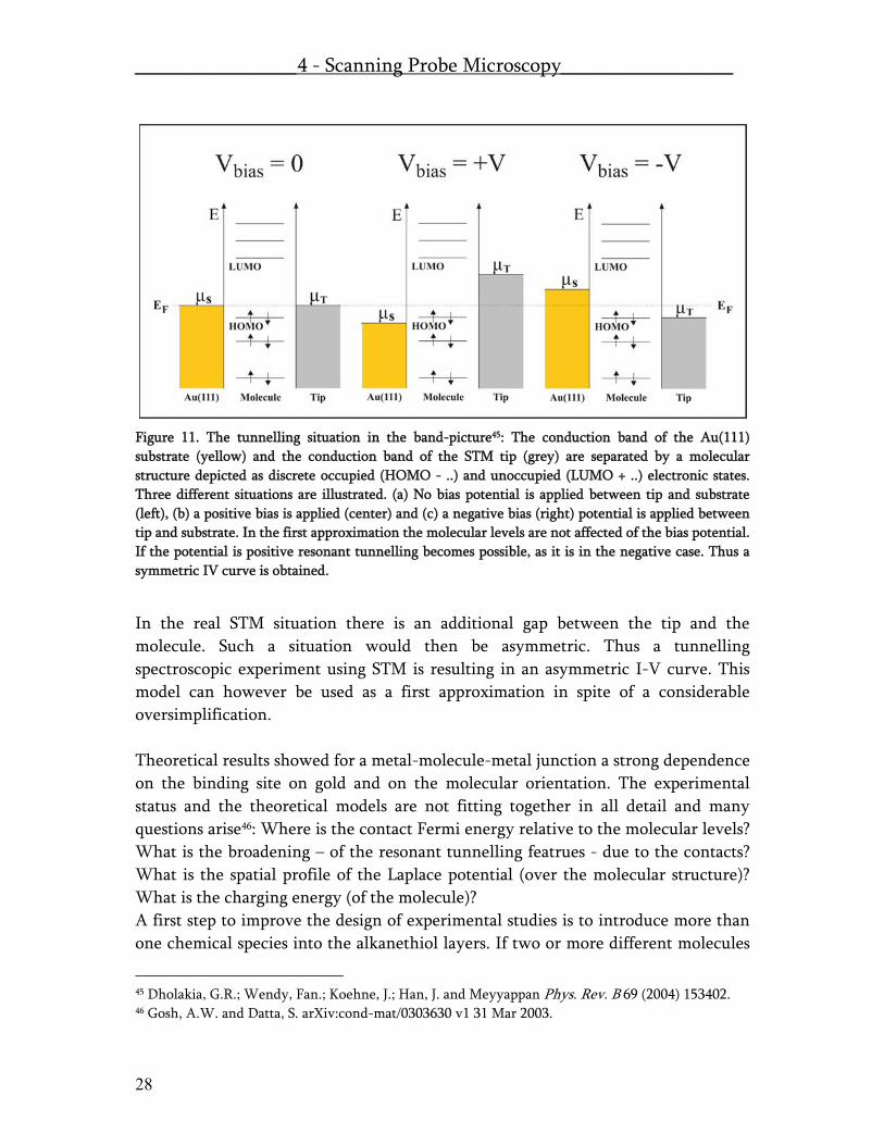
Figure 11. The tunnelling situation in the band-picture45: The conduction band of the Au(111) substrate (yellow) and the conduction band of the STM tip (grey) are separated by a molecular structure depicted as discrete occupied (HOMO - ..) and unoccupied (LUMO + ..) electronic states. Three different situations are illustrated. (a) No bias potential is applied between tip and substrate (left), (b) a positive bias is applied (center) and (c) a negative bias (right) potential is applied between tip and substrate. In the first approximation the molecular levels are not affected of the bias potential. If the potential is positive resonant tunnelling becomes possible, as it is in the negative case. Thus a symmetric IV curve is obtained.
In the real STM situation there is an additional gap between the tip and the molecule. Such a situation would then be asymmetric. Thus a tunnelling spectroscopic experiment using STM is resulting in an asymmetric I-V curve. This model can however be used as a first approximation in spite of a considerable oversimplification. Theoretical results showed for a metal-molecule-metal junction a strong dependence on the binding site on gold and on the molecular orientation. The experimental status and the theoretical models are not fitting together in all detail and many questions arise46: Where is the contact Fermi energy relative to the molecular levels? What is the broadening – of the resonant tunnelling featrues - due to the contacts? What is the spatial profile of the Laplace potential (over the molecular structure)? What is the charging energy (of the molecule)? A first step to improve the design of experimental studies is to introduce more than one chemical species into the alkanethiol layers. If two or more different molecules
45 Dholakia, G.R.; Wendy, Fan.; Koehne, J.; Han, J. and Meyyappan Phys. Rev. B 69 (2004) 153402. 46 Gosh, A.W. and Datta, S. arXiv:cond-mat/0303630 v1 31 Mar 2003.
________________4 - Scanning Probe Microscopy_________________
29
can be introduced into a layer and be identified one has the possibility to relatively measure conductivity on two molecular systems using the same tip. An additional experimental advancement consists in the introduction of a different binding group. One theoretical model can now be applied to simulate two binding groups and thus the experimentally detectable relative conductivity difference can be determined.
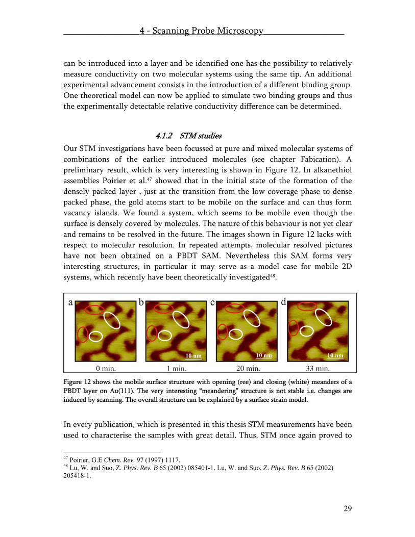
4.1.2 STM studies Our STM investigations have been focussed at pure and mixed molecular systems of combinations of the earlier introduced molecules (see chapter Fabication). A preliminary result, which is very interesting is shown in Figure 12. In alkanethiol assemblies Poirier et al.47 showed that in the initial state of the formation of the densely packed layer , just at the transition from the low coverage phase to dense packed phase, the gold atoms start to be mobile on the surface and can thus form vacancy islands. We found a system, which seems to be mobile even though the surface is densely covered by molecules. The nature of this behaviour is not yet clear and remains to be resolved in the future. The images shown in Figure 12 lacks with respect to molecular resolution. In repeated attempts, molecular resolved pictures have not been obtained on a PBDT SAM. Nevertheless this SAM forms very interesting structures, in particular it may serve as a model case for mobile 2D systems, which recently have been theoretically investigated48.
Figure 12 shows the mobile surface structure with opening (ree) and closing (white) meanders of a PBDT layer on Au(111). The very interesting “meandering” structure is not stable i.e. changes are induced by scanning. The overall structure can be explained by a surface strain model.
In every publication, which is presented in this thesis STM measurements have been used to characterise the samples with great detail. Thus, STM once again proved to
47 Poirier, G.E Chem. Rev. 97 (1997) 1117. 48 Lu, W. and Suo, Z. Phys. Rev. B 65 (2002) 085401-1. Lu, W. and Suo, Z. Phys. Rev. B 65 (2002) 205418-1.

________________4 - Scanning Probe Microscopy_________________
30
be a powerful tool. Here it is used to probe pure dithiocarbamate systems, mixed assemblies and molecular gradients.
4.2 Atomic Force Microscopy (AFM) The atomic force microscope (AFM), or scanning force microscope (SFM) was invented and introduced in 1986 by Binnig, Quate and Gerber49. The AFM, like its predecessor, the STM was undergoing a fast development in the year after the first presentation. The micro-mechanical cantilever and the position read-out mechanism changed and lead to a variety of different modes how to use and drive an AFM (see Figure 13). In the field of molecular assemblies on metallic and non metallic surfaces i.e. for the study of self-assembled monolayers two AFM techniques are favoured – the contact mode and the lateral force mode. Scanning at environmental conditions on surfaces suffers always from the water layer which is abundant on almost every surface. As shown in Figure 14 this thin layer can eliminate the possible locality of the tip substrate (molecule) interaction. The water layer can form a liquid neck50 and even if it’s not as stable as shown in the drawing (Figure 14) the additional potential is smearing out the local definition of the tip substrate interaction. If we add a liquid, preferentially a hygroscopic solvent like dry ethanol we can significantly reduce this potential problem. If the water cannot be removed totally from the surface by the ethanol and the scanning tip still dips into the water layer the problem is almost solved. The strongest contribution to the disturbing potential originates from the surface tension of the water layer, which is effectively lowered by the surrounding ethanol. In the case of a pure alkanethiol monolayer no water is on adsorbed on the surface due to the highly unpolar alkane chains forming the outhermost layer structure. AFM scanning under ethanol resulted in much higher resolution than on air. This might be due to the reduced van der Waals attraction between tip and surface if an additional dielectric media is present.
49 Binnig, G.; Quate, C.F. and Gerber, Ch. Phys. Rev. Lett. 56 (1986) 930. 50 Luna, M.; Colchero, J. and Baró Appl. Phys. Lett. 72 (1998) 3461.

________________4 - Scanning Probe Microscopy_________________
31
Figure 13 shows the set-up of an atomic force microscope (AFM). The same positioning system as implemented in the STM (piezo-crystal (5), feedback control (6)) is used in AFM. By using a microfabricated cantilever (2) the local sample (4) surface structure can be mechanically probed. The cantilever is scanned over the surface and the modulation of the tip by the surface is determined by a laser positioning system. The laser beam (1) is pointing on the lever right above the tip and the reflection is red out by a quadrant detector (3). This system is suitable to measure the height modulation as well as the lateral bending of the lever, which can be related to the local friction interaction.

________________4 - Scanning Probe Microscopy_________________
32
The first AFM studies, which could get molecular resolved images on alkanethiolate layers however, were performed under ambient conditions51. Different kinds of molecular defects and packing structures were found by scanning under liquids52. An interesting experiment was done by Gang-yu Liu et al.53. Molecular distances have here been imaged at low loads, and have been attributed to the decanethiolate SAM, whereas at high loads a smaller lattice constant was imaged and attributed to the underlying gold substrate. By lowering the load to the initial value the measured lattice distance fitted to the initial measurement again. Other studies measured friction54 or elasticity55 on pure SAMs. Friction properties have also been tested on low coverage SAM phases56. In-situ adsorption of thiols on gold were perfomed on Octadecanethiols57 (long chains ideally crystallising) and on mixed58 (decanethiol/hexadecanethiol) SAM systems using AFM. Interesting to our mixed systems approach are the results, which could be obtained by Nelles et al. scanning over SAMs formed by asymmetrical diethylalkanoat disulfides59. In this system does no phase separation occur and even though molecular resolution could be measured applying force typically 1 nN. This indicates that the scanning tip is penetrating into the SAM for about 4-8Å. In a continuative very detailed study they found interesting details by 2D FT analysis and they determined in this latter assessment the same penetration depth60.
4.2.1 AFM and LFM on thiol SAMs The first steps in order to explore molecular thiol assemblies on Au(111) were AFM measurements on octanethiol SAMs. The first experiments under ambient conditions did not reveal any insight into these layers.
51 Alves, C.A.; Smith, E.L. and Porter, M.D. J. Am. Chem. Soc. 114 (1992) 1222. 52 Butt, H.-J.; Seifert, K. and Bamberg, E. J. Phys. Chem. 97 (1993) 7316. 53 Liu G-y. and Salmeron, M.B. Langmuir 10 (1994) 367. 54 Kim, Y.; Kim, K.-S.; Park, M. and Jeong, J. Thin Solid Films 341 (1999) 91. Bhushan, B. and Liu, H. Phys. Rev. B 63 (2001) 245412. Brewer, N.J.; Foster, T.T.; Leggett, G.J.; Alexander, M.R. and McAlpine, E. J. Phys Chem. B 108 (2004) 4723. 55 Domke, J. and Radmacher, M. Langmuir 14 (1998) 3320. 56 Zhang, C.; Liang, Q.; Wang, B. and Xiao, X. J. Appl. Phys. 95 (2004) 3411. 57 Xu, S.; Cruchon-Dupeyrat, S.J.N.; Garno, J.C.; Liu, G-Y.; Jennings, G.K.; Yong, T.H. and Laibinis, P.E. J. Chem. Phys. 108 (1998) 5002. 58 Barrena, E.; Ocal, C. and Salmeron, M. Surf. Sci. 482 (2001) 1216. 59 Nelles, G.; Schönherr, H.; Vansco, G.J. and Butt, H.-J. Appl. Phys. A 66 (1998) 1261. 60 Nelles, G.; Schönherr, H.; Jaschke, M.; Wolf, H.; Schaub, M.; Küther, J. Tremel, W.; Bamberg, E.; Ringsdorf, H.; Butt, H.-J. Langmuir 14 (1998) 808.

________________4 - Scanning Probe Microscopy_________________
33
Figure 14 is showing the tip substrate interaction in two different cases. Scanning under ambient conditions (air) is shown on the right side. The tip is attracted by van der Waals forces61 to the substrate (c). On the right side scanning under ethanol (d) is sketched and there is no van der Waals attraction occurring anymore. Under lower tip sample attraction the adlayer (b) structure can be imaged more accurately.
The next experiments were done under liquids. Ethanol was the liquid of choice because of the good solubility of water and thiols. In literature the in-situ adsorption of octadecanethiol was described62. It seemed to be possible to detect the outermost methyl group because in that study the tilting angle of the molecules (as know from many other measurements 30-35°) was determined using the AFM detected layer thickness. Our in-situ adsorption experiments were performed in a liquid cell as shown in Figure 33. The results an in-situ adsorption experiment of octanethiol on Au(111) is shown in Figure 16. In the first row (1a-1d) a series of lateral force micrographs are shown. The evolution over time of the thiol ad-layer is clearly visible. The information provided by the height signal was not sensitive enough to prove the adsorption of the layer. Even though it was possible in the beginning of the experiment to resolve the atomic gold structure (2a). After the assembly process 61 J. Israelachvili, Intermolecular and Surface Forces Academic Press, London, 1991. 62 Liu, G-Y.; Xu, S. and Cruchon-Dupeyrat, S. in Ulman A. (Ed) „SELF-ASSEMBLED MONOLAYERS OF THIOLS“ Thin Film Volume 24, Academic Press, San Diego, USA, 1998.

________________4 - Scanning Probe Microscopy_________________
34
it was also possible to detect the well-known etch-pits on the gold surface (height singal, 2b) and the molecular spacing of the octanethiol SAM was determined to be 0.5 nm (2c). This result was very promising and we started to explore mixed SAMs. Our collaborators from Sony (Sony Stuttgart Technology Center, Materials Science Laboratories) gained experimental experience in fabricating and imaging (STM) mixed SAMs consisting of DMAAB and octanethiol. We followed the recommended proceeding protocol to form mixed molecular layers. The resulting sample should simultaneously expose on the surface low coverage thiol phase, standing octanethiol phase and islands consisting of DMAAB. The AFM analysis was again performed under ethanol in the liquid cell.
Figure 15 shows the used AFM liquid cell set-up (Multimode AFM from Digital Instruments). The liquid cell allows us to investigate in-situ adsorption of molecules on surfaces. The cantilever can be mounted on a insulated spring (1) and is controlled by a laser read out system (4). The sealing silicon ring (2) allows the piezo and the sample to move under the fixed cantilever and obturates the liquid filled volume. First the volume is filled by ethanol trough the in- and out-let (3) and the liquid used to flush the cell is collected in the container (6). After the flushing the syringe was changed from a pure ethanol filling to a thiol containing filling and the solution was introduced to the liquid cell, which was followed by the adsorption of the molecules on the surface.

________________4 - Scanning Probe Microscopy_________________
35
Figure 16. In-situ adsorption experiment of octanethiol on Au(111) monitored by lateral force microscopy. Octanethiol (OT) was diluted in ethanol and introduced into the liquid cell. The red square indicates the same region on the surface in the picture series 1a-1d (1a,1b: 1,3×1,3 μm2; 1c,1d: 2.5×2.5 μm2). Picture 2a shows atomar resolution of the initial gold surface before introducing OT. After the whole adsorption experiement the well known etch-pits could be detected and the molecular distance was determined to be 0.5 nm.
The results of these AFM/LFM scans are shown in Figure 8. We could detect low coverage (first time by AFM) but astonishingly no islands and other contrasts could be detected. These data showed that the tip was penetrating into the layer especially in the case of the “soft” octanethiol SAMs. The determination of the penetration depth (illustrated in Figure 17) is in very good agreement with the findings of Nelles (cited above). So we decided not to use AFM in the further proceedings because we proofed that the AFM tip was penetrating into the SAM and we were not able to image the outermost methyl ends of the thiol layers.

________________4 - Scanning Probe Microscopy_________________
36
Figure 17 shows AFM results obtained at LMN/PSI. On top we see molecular resolved low coverage phase of octanethiol (1a height, 1b friction, 1c length and 1d molecular distance) on a mixed octanethiol/DMAAB sample. From STM experiments we know that on this surface ordered thiol domains as islands of DMAAB must be present. As we show low coverage phase on a mixed DMAAB/DT SAM. The friction mode scan (1b) is showing more details of the surface structures than the height mod.

37
5 Cyclic Voltammetry Cyclic Voltammetry (CV) is a widely used electrochemical technique63,64. The first experiments using cyclic voltammetry in the field of self-assembled monolayers have been done by Porter et. al65. and showed that redox currents of the [Fe3+(CN-)6] redox system could be efficiently blocked. The demonstrated redox-current inhibition was strongly depending on the chain length of the assembled alkanethiols (C4, C8 and C12) on the polycrystalline gold electrode. These technique were used in different ways e.g. to determine the temperature dependent phase transition and the density of assembled layers and to show that days to weeks of assembly time are needed to end-up with a current inhibiting, low defect density SAM66. Widrig et al.67 directly studied the surface oxidation/reduction processes of thiol SAMs and identified the oxidative and reductive desorption processes from the surface. They used well characterised flat gold surfaces (gold evaporated on mica followed by an additional annealing step) and assembled the investigated thiols from ethanolic solution. A good agreement between the reductive (and oxidative!) charge and the molecular density calculated from the earlier result was found (alkanethiols assemble in a ( ) °× 3033 R structure on Au(111) surfaces). Finally they found the following relation in quantitative analysis of their data:
AuS(CH2)nCH3 + e- = Au(0) + -S(CH2)nCH3. (2)
These experiments were carried out in 0.5 KOH solution at a voltage scan rate of 100mV/s. After these first achievements, other groups compared the IR absorption of bound and unbound Au-thiol complexes, the oxidative/reductive charge of
63 Holze, R. Leitfaden der Elektrochemie G.Teubner, Stuttgart, 1998. 64 Bard, A.J. Electrochemical Methods : Fundamentals and Applications John Wiley & Sons. New York, 2nd edition, 2000. 65 Porter, M.D.; Bright, T.B.; Allara, D.L. and Chidsey, C.E.D. J. Am. Chem. Soc. 109 (1987) 3559. 66 Badia, A.; Back, R. and Lennox, R.B. Angew. Chem. Int. Ed. Engl. 33 (1994) 2332. 67 Widrig, C.A.; Chung, C. and Porter M.C. J. Electoanal. Chem. 310 (1991) 335.
___________________5 - Cyclic Voltammetry____________________
38
Ferrocenes attached by a thiol group to the gold surface and the reductive desorption charge. All these experiments confirmed to this equation68. Walczak et al. have shown that the reductive desorption process on terraces energetically differs from the desorption process at step edges (butanethiol, octanethiol). This was achieved by comparing samples with increasing corrugation and step density: Au/mica, Au/glass and Au/Si from the former to the latter and by finding a two peak desorption behaviour with corresponding changes in the peak heights found in CV.69 In a second important experiment the same authors assigned most of the gold surface area to consist of Au(111) facets by comparing the iodine and Pd adsorption. Iodine adsorbs at every gold site whereas Pb can be selectively be adsorbed at Au(111) sites. The ratio of the amount of adsorbed I and Pb determines the ratio of total gold surface to Au(111) facets. In more detail, the reductive desorption is not only sensitive to the adsorption site of the thiolates, but it depends also on the 2d packing within the molecular layer70 and on pH71.
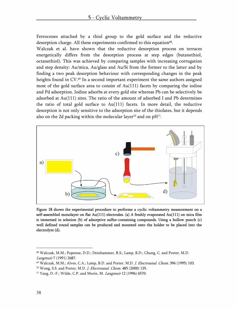
Figure 18 shows the experimental procedure to performe a cyclic voltammetry measurement on a self-assembled monolayer on flat Au(111) electrodes. (a) A freshly evaporated Au(111) on mica film is immersed in solution (b) of adsorptive sulfur-containing compounds. Using a hollow punch (c) well defined round samples can be produced and mounted onto the holder to be placed into the electrolyte (d).
68 Walczak, M.M.; Popenoe, D.D.; Deinhammer, R.S.; Lamp, B.D.; Chung, C. and Porter, M.D. Langmuir 7 (1991) 2687. 69 Walczak, M.M.; Alves, C.A.; Lamp, B.D. and Porter, M.D. J. Electroanal. Chem. 396 (1995) 103. 70 Wong, S.S. and Porter, M.D. J. Electroanal. Chem. 485 (2000) 135. 71 Yang, D.-F.; Wilde, C.P. and Morin, M. Langmuir 12 (1996) 6570.
___________________5 - Cyclic Voltammetry____________________
39
In our experimental set-up we use a Hg/HgO [OH-] reference electrode. A stainless steel wire sample holder has been built, electrochemically plated with 3 μm gold and bent into a clamping spiral (see Figure 18) prior to the experiments. This spiral supports the punched mica sample with the SAM gold layer as shown in Figure 1. We use 0.5 M KOH as electrolyte. The electrolyte was de-aerated by bubbling nitrogen through it for 20 min. Usually the applied potential scan rate was 50 mV/s. A typical record of a reductive desorptive cyclic voltammogram is shown in Figure 19. In this Figure four regions of the voltammetric scan are labelled (a) to (d) for each cycle. In every region one can see a small sketch of the corresponding situation on the gold surface i.e. whether the molecules stick to the surface or not. In region (a), above the desorptive potential, all the molecules are still bound to the surface. The red curve shows the first voltammetric cycle of the experiment. By lowering the electrochemical potential to a certain extent a strong peak in the desorption current can be measured. This peak is assigned to the reductive desorption of the full monolayer. After reaching –1300 mV v.s. Hg/HgO [OH-] the potential is swept back to the initial potential. In region (b) and (c) the molecules are completely released from the surface and start to diffuse away from the surface. As diffusion is a rather slow process a significant fraction of the thiol can be re-adsorbed, which is occurring at a potential of about –920 mV where a small but distinct peak appears. In region (d) the rest of the molecules in reach of the surface re-adsorb to the surface and stay there until the potential is lowered below the desorption potential.

___________________5 - Cyclic Voltammetry____________________
40
Figure 19. The first two cycles of a reductive desorption experiment of a dense octanethiol layer from a evaporated Au(111) electrode on mica. The integral of the first cycle (area denoted in red) provides a measure of the total charge involved in the layer desorption. The second cycle (blue) shows a more pronounced two peak behaviour than the first (red) cycle. This is the typical case for a well established ‘standing’ layer which re-forms only partially under concurrent formation of ‘lying’ low density phases after complete desorption in the first cycle.
In the second cycle (blue) the desorption occurs at the same potential as in the first one, and the lower desorption peak corresponds to the partial re-adsorption of the molecules forming the initial monolayer. The re-adsorption in the second (blue) curve is further decreased by a certain fraction of molecules which have been diffusing away from the sample into the solution. Consequent to continuous sweeping the desorption and re-adsorption peaks are lowered until they diminish (after ~10 cycles). These experiments provide clear evidence for reductive desorption processes and for the formation of the molecular layers by ‘chemisorption’ to the substrate.. The first current peak can be taken as a measure of surface coverage as these molecules need one electron to desorb. We can calculate the number of electrons involved in the desorption process by integrating the area under the peak (red area in Figure 19) and by dividing it by the scan rate (Q = (I/U)/(U/t)=I×t). The peak area or desorption ‘charge’ has also been used as a measure for the adsorption

___________________5 - Cyclic Voltammetry____________________
41
kinetics of decanethiol72. It has been shown that different chain length of alkanethiols result in different desorption potentials73 and that single components in mixed monolayers of ω-substituted alkanethiols can be separately detected in an electrochemical desorption experiment. Thus, phase separation can be analysed in detail74,75. Additionally it is possible to set the potential close to the threshold for desorption of one species in a mixed monolayer and study the partial desorption. Taking out the sample at the applied potential and re-immersion it into a thiol solution the selective replacement, with respect to potential surface patterning76,77 can be tested. Others investigated mercapto aminophenol assemblies by means of CV in combination with STM and XPS. For aromatic thiols two reductive desorption peaks separated by several hundred millivolts were found and attributed to compact (standing) and low density (flat lying) molecular islands of the phenyl ring containing molecules78. In our investigation using dithiols: BDMT and DMAAB, we found very different behaviours depending on the assembly time of the molecules. DMAAB is going through many different states of organisation (three peak behavour!) while for BDMT only after a very short assembly time two peaks (small) could be detected. The results of a long time assembled monolayer of DMAAB and BDMT showed two peaks for DMAAB and one peak for BDMT. The total charge used for this desorption is almost the same (see table 5). In our experiments we successfully confirm that the reductive desorption for adsorbed thiols from gold is a one electron process. Theoretically a ( ) °× 3033 R structured monolayers (7.6 10-10 mol/cm2) correspond to a desorption charge desitiy of 0.73 μC/mm2. We found (see Table 1), in agreement with the majority of the previous studies, slightly enhanced desorption charge densities. This is usually attributed to an influence of the surface roughness. The previously described trend for alkanethiols - the longer the alkyl chain the lower the desorption potential – was also confirmed in our investigations (C8 at –1055 mV, C10 at –1125 mV and C12 at – 1201 mV).
72 Sumi, T.; Wano, H. and Uosaki, K. J. Electroanal. Chem. 550-551 (2003) 321. 73 Kakiuchi, T.; Usui, H.; Hobara, D. and Yamamoto, M. Langmuir 18 (2002) 5231. 74 Hobara, D.; Ota, M.; Imbayashi, S.-i.; Niki, K. and Kakiuchi, T. J. Electroanal. Chem. 444 (1998) 113. 75 Kakiuchi, T.; Sato, K.; Iida, M.; Hobara, D.; Imbayashi, S.-i. and Niki. K. Langmuir 16 (2000) 7238. 76 Imbayashi, S.-i.; Hobara, D. and Kakiuchi, T. Langmuir 13 (1997) 4502. 77 Hobara, D.; Sasaki, T.; Imbayashi, S.-i. and Kakiuchi, T. Langmuir 15 (1999) 5073. 78 Batz, V.; Schneeweiss, M.A.; Kramer, D.; Hagenström, H.; Kolb, D.M. and Mandler, D. J. Electroanal. Chem. 491 (2000) 55.

___________________5 - Cyclic Voltammetry____________________
42
The sulfur content on the other molecular assemblies has been determined by XPS because STM can not image all molecular systems with molecular resolution. By comparison of the relative sulfur content to the alkanethiol data we calculate the absolute sulfur content on the surface.
Table 5 shows the reductive desorption charges measured for all used molecules in our studies.
CV Signalsa)
CompoundPotential
of DesorptionCharge
[μC/mm2]Octanethiol -1055(15) 0.80(6)Decanethiol -1125(5) 0.83(1)Dodecanethiol -1201(7) 0.70(5)BDMT -1041(5) 0.94(4)DMAABb) -1028(9) 0.92(15)DEDT -791(18) 0.60(10)APDC -804(10) 1.00(15)Thiram -759(8) 0.85(10)cHBDT -1023(12) 1.83(13)PBDT -1012(6) 1.95(11)
a). Main Peak of the CV signal, charge total reductive charge. b). DMAAB showed a very interesting assembly time dependent CV characteristic. Usually showing more than one peak! The new functional group, which has been introduced as a SAM forming system in this thesis is the dithiocarbamate group. A similar group, the xanthic acids and the dithiocarbamates have been used to fabricate SAMs since the early days of research on the thiol-on-gold assembly79,80. The dithiocarbamates form no ideal layers, as it has been tested by contact angle measurements. The xanthic acids have been observed to form densely packed molecular layers. Reductive desorption was tested for xanthic acids81 (only qualitatively) but no study used dithiocarbamate assembled on gold (metal) to investigate the desorption properties qualitatively and quantitatively. In our study on the monodithiocarbamates (DEDT, APDC and Thiram – assembles in the same structure as a dithiocarbamate) it is concluded that the following relation holds:
AuS2R + e- = Au(0) + -SSR (3)
79 Bain, C.D.; Evall, J. and Whitesides, G.M. J. Am. Chem. Soc. 111 (1989) 7155. 80 Arndt, Th.; Schupp, H. and Schrepp, W. Thin Solid Films 178 (1989) 319. 81 Gothelf, K.V. J. Electroanal. Chem. 494 (2000) 147.

___________________5 - Cyclic Voltammetry____________________
43
Thus, one electron is needed for each molecular desorption process. In the desorption process of bisdithiocarbamates (cHBDT and PBDT) more electrons per molecule are involved, an observation which we tentatively assign to a destructive desorption process on the basis of the small CV detectable re-adsorption peak (see publication in this thesis “Dithiocarbamate and thiurame re-visited”).


45
6 Near Edge X-Ray Absorption Fine Structure (NEXAFS)
Near edge X-Ray absorption fine structure is a synchrotron based surface sensitive analysis method. In order to measure the X-ray absorption depending on the incoming photon energy it is a requirement to scan the photon energy. Additionally chiral and/or magnetic phenomena can be explored by analysing the polarisation dependence of a NEXAFS experiment. Synchrotron radiation is polarized by its nature. The Swiss Light Source (SLS) – located at the Paul Scherrer Institute (PSI) is a third generation synchrotron driven in the continous electron re-fill mode and running at a permanent current of 300 mA. All our experiments were carried out at the Surface /Interface Materials Beamline (SIM). 6.1 X-Ray Absorption – Theory Our investigations of thiol and dithiocarbamate molecules on gold surfaces were exclusively performed at the carbon K-edge. Thus, we detected photelectrons originating from X-ray absorption processes in the photon energy range of 270-330 eV which is the required energy range to excite the C1s electron into unoccupied molecular orbitals, into vacuum continuum states or directly into free vacuum states. As shown in the energy level diagram in Figure 20, absorption peaks are corresponding to each of these possible electron transitions. In Figure 22 the spatial situation of an electron excitation process from occupied to unoccupied molecular orbitals is illustrated. The theoretical treatment of NEXAFS82 usually starts with a first approximation using Fermi’s “Golden Rule”, which allows us to calculate the transition probability of a quantum system from the initial state i to the final state f driven by a time
dependent periodic perturbation ( ) tieVtV ω= , which is appropriate in the case of a photon absorption process. The transition probability is given by
82 J. Stöhr; NEXAFS Spectroscopy, Springer Series in Surface Science 25, Springer Berlin, Second Printing 2003
__________6 - Near Edge X-Ray Absorption Fine Structure_________
46
( )EiVfP fif ρπ 22h
= , (4)
where ( )Efρ is the energy density of the final states. In order to get the full x-ray absorption cross section (σx) at a given photon energy we have to sum over all atomic shells with binding energies below ωh . As we are mainly interested in the inner shells and the outer shells have a smooth cross section at inner-shell excitation energies we ignore for simplicity the contribution of the outer shells to the total cross section. If we apply the dipol approximation and use coordinates in space we end up with the following expression:
( )EixEfP fifx ρσ 2•∝∝ . (5) Here we see that the angle between the polarisation direction of the incident light ( E ) and the position of the excited electron ( x ) plays an important role with respect to the absorption intensity. For the discussion of the angular dependence of the K-shell resonances usually the molecules i.e their bonds are classified into general groups. The classification is based on the high directionality of molecular bonds and the related molecular orbitals (MOs). K-shell excitation spectroscopy is a localised spectroscopy that probes the amplitude and directionality of the excited state MOs on the excited atom. Only the spatial orientation of the orbital, i.e., the direction of maximum orbital amplitude, determines the angular dependence of the K-shell spectra. Therefore we can represent a single orbital by a vector, and two orthogonal orbitals (or several orbitals in one plane) by a plane.
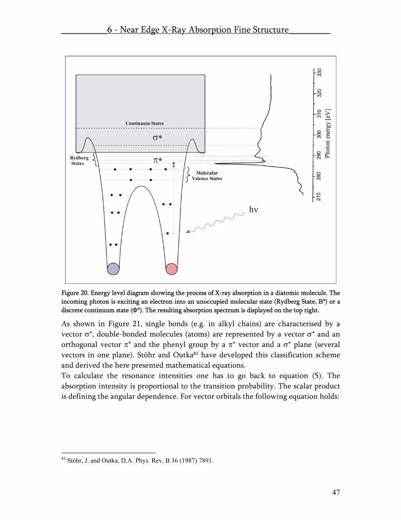
__________6 - Near Edge X-Ray Absorption Fine Structure_________
47
Figure 20. Energy level diagram showing the process of X-ray absorption in a diatomic molecule. The incoming photon is exciting an electron into an unoccupied molecular state (Rydberg State, Β*) or a discrete continuum state (Φ*). The resulting absorption spectrum is displayed on the top right.
As shown in Figure 21, single bonds (e.g. in alkyl chains) are characterised by a vector σ*, double-bonded molecules (atoms) are represented by a vector σ* and an orthogonal vector π* and the phenyl group by a π* vector and a σ* plane (several vectors in one plane). Stöhr and Outka83 have developed this classification scheme and derived the here presented mathematical equations. To calculate the resonance intensities one has to go back to equation (5). The absorption intensity is proportional to the transition probability. The scalar product is defining the angular dependence. For vector orbitals the following equation holds:
83 Stöhr, J. and Outka, D.A. Phys. Rev. B 36 (1987) 7891.

__________6 - Near Edge X-Ray Absorption Fine Structure_________
48
δ2cos∝VI , (6)
where δ stands for the angle between the polarisation direction of the incoming x-ray and the direction between the C1s ( i ) state and the final orbital state ( f ). For plane orbitals we get the relation:
ε2sin∝pI , (7)
where ε stands for the angle between the polarisation direction of the incoming x-ray and the normal of the plane. To derive the final expression for the angle dependent absorption intensity one has to take the substrate symmetry into account. Figure 23 shows the two different situations: (a) the vector case and (b) the plane case. The mathematical expressions for the angular dependence of a threefold symmetric substrate is given by:
Figure 22. Real space situation of the excitation process from the C1s state to the Lumo+1. As the unoccupied molecular orbitals are not homogeniously distributed around the molecular backbone the excitation from the spherical symmetric C1s level into a molecular orbital is directional i.e polarisation dependent.
Figure 21. Ilustration of spatial orientation of π* and σ* orbitals in the three important groups of molecules for this thesis. The single bond configuration a), the double bond configu-ration b) and the aromatic ring configuration c).
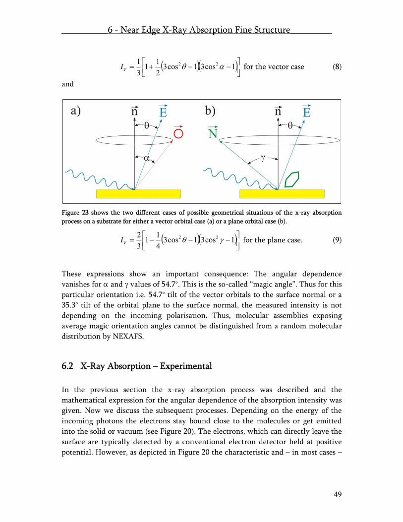
__________6 - Near Edge X-Ray Absorption Fine Structure_________
49
( )( )⎥⎦⎤
⎢⎣⎡ −−+= 1cos31cos3
211
31 22 αθVI for the vector case (8)
and
Figure 23 shows the two different cases of possible geometrical situations of the x-ray absorption process on a substrate for either a vector orbital case (a) or a plane orbital case (b).
( )( )⎥⎦⎤
⎢⎣⎡ −−−= 1cos31cos3
411
32 22 γθVI for the plane case. (9)
These expressions show an important consequence: The angular dependence vanishes for α and γ values of 54.7°. This is the so-called “magic angle”. Thus for this particular orientation i.e. 54.7° tilt of the vector orbitals to the surface normal or a 35.3° tilt of the orbital plane to the surface normal, the measured intensity is not depending on the incoming polarisation. Thus, molecular assemblies exposing average magic orientation angles cannot be distinguished from a random molecular distribution by NEXAFS.
6.2 X-Ray Absorption – Experimental In the previous section the x-ray absorption process was described and the mathematical expression for the angular dependence of the absorption intensity was given. Now we discuss the subsequent processes. Depending on the energy of the incoming photons the electrons stay bound close to the molecules or get emitted into the solid or vacuum (see Figure 20). The electrons, which can directly leave the surface are typically detected by a conventional electron detector held at positive potential. However, as depicted in Figure 20 the characteristic and – in most cases –

__________6 - Near Edge X-Ray Absorption Fine Structure_________
50
most significant NEXAFS information originates from processes below the energy range allowing for direct emission processes. After the initial excitation of the molecules competing relaxation processes are taking place. As mentioned in the beginning of this chapter measuring at the K-edge means that electrons are excited out of the 1s state. Thus, all the other electrons of the molecules (except the remaining 1s electron) can relax into the free 1s state by emitting a photon ( fi EE −=ωh ). This photon can in principal be emitted (luminescence) but
usually the photon excites another, outer shell electron into emission. Such electrons are called Auger electrons and the whole process is called Auger process. (see chapter XPS). A pre-existing hole in the K-shell is predominantly followed by an Auger process 84 for the light elements – from lithium to sodium no photoemission occurs. These distinctively different mechanisms for electron emission allow us to select one of three possible methods to detect the photon energy dependent electron flow. The three methods are: Auger electron yield (AEY), partial electron yield (PEY) and total electron yield (TEY). To measure the AEY and PEY one has to use an electron detector set-up to measure directly the electrons, which are escaping from the surface. To detect only the Auger electrons (AEY) one has to eliminate electrons with to higher energies (direct emission of outer shell electrons) i.e. set a maximal acceptance energy. To work in the PEY one has to introduce additionally a minimal acceptance limit and as the name indicates the TEY (total electron yield) does not exclude any electrons. In our investigations we measured the TEY, therefore we used an ampere-meter to determine the current flowing back to the sample depending on the incoming photon energy as shown in Figure 24.
84 M. Henzler and W. Göpel; Oberflächenphysik des Festkörpers, B.G. Teubner Stuttgart 1994.
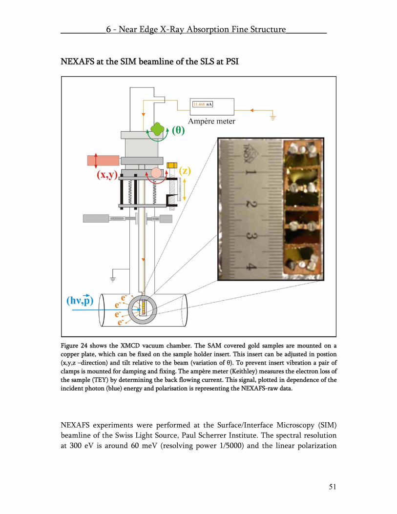
__________6 - Near Edge X-Ray Absorption Fine Structure_________
51
NEXAFS at the SIM beamline of the SLS at PSI
Figure 24 shows the XMCD vacuum chamber. The SAM covered gold samples are mounted on a copper plate, which can be fixed on the sample holder insert. This insert can be adjusted in postion (x,y,z –direction) and tilt relative to the beam (variation of θ). To prevent insert vibration a pair of clamps is mounted for damping and fixing. The ampère meter (Keithley) measures the electron loss of the sample (TEY) by determining the back flowing current. This signal, plotted in dependence of the incident photon (blue) energy and polarisation is representing the NEXAFS-raw data.
NEXAFS experiments were performed at the Surface/Interface Microscopy (SIM) beamline of the Swiss Light Source, Paul Scherrer Institute. The spectral resolution at 300 eV is around 60 meV (resolving power 1/5000) and the linear polarization

__________6 - Near Edge X-Ray Absorption Fine Structure_________
52
degree is 100%. The orientation of the linearly polarized X-rays can be varied between 0 and 90 degree in steps of 5° enabling the measurement of orientation effects without the need to rotate the sample. The geometric situation of the polarisation direction and the tilted sample with respect to the incident beam is shown in Figure 25. The NEXAFS spectra were taken with the total electron yield (TEY) detection, which is ideally suited for the measurement of thin films due to the small electron escape depth of typically less than a few nm. The samples were mounted in the XMCD vacuum chamber, which is not at the focus point of the beamline resulting in spot size of approximately (0.3 * 1.5) mm (tilted sample results in elliptic spot!). The TEY signal was obtained by measuring the sample photocurrent with a pico-ampère-meter (Keithley) and by typically normalising it to the intensity of the incident photon beam as measured by the photocurrent of the Pt coating of the last mirror (i.e. a reference for the initial beam-intensity). This photocurrent was measured in every run. However, due to contamination problems the normalisation using this mirror signal was not always suitable.
Figure 25. Geometric situation of the incoming X-ray beam and the polarisation direction relative to the sample surface. By changing the beam polarisation the angle between the surface and the polarisation is changing. The equation describes the relations of these values.
Surface sensitive investigations by X-ray Absorption measurements, in particular those measuring carbon compounds or monolayer thin samples have to carefully
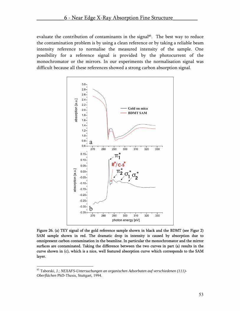
__________6 - Near Edge X-Ray Absorption Fine Structure_________
53
evaluate the contribution of contaminants in the signal85. The best way to reduce the contamination problem is by using a clean reference or by taking a reliable beam intensity reference to normalise the measured intensity of the sample. One possibility for a reference signal is provided by the photocurrent of the monochromator or the mirrors. In our experiments the normalisation signal was difficult because all these references showed a strong carbon absorption signal.
Figure 26. (a) TEY signal of the gold reference sample shown in black and the BDMT (see Figur 2) SAM sample shown in red. The dramatic drop in intensity is caused by absorption due to omnipresent carbon contamination in the beamline. In particular the monochromator and the mirror surfaces are contaminated. Taking the difference between the two curves in part (a) results in the curve shown in (c), which is a nice, well featured absorption curve which corresponds to the SAM layer. 85 Taborski, J.; NEXAFS-Untersuchungen an organischen Adsorbaten auf verschiedenen (111)-Oberflächen PhD-Thesis, Stuttgart, 1994.

__________6 - Near Edge X-Ray Absorption Fine Structure_________
54
One technical solution to avoid such problems is to freshly evaporate gold just before the measurement in-situ onto a gold mesh, which can be positioned into the beam during the measurement. The photocurrent of this mesh can then be used as normalisation signal. This set-up was not easy to implement at the SIM beamline, therefore we used freshly evaporated gold films in the same quality and thickness as used for SAM fabrication. These films were cleaned in a UV/Ozone cleaner right before mounting the samples into the vacuum chamber. The UV/Ozone cleaner was supposed to remove all contaminants from the surface. In the short time periode between removing the sample from the UV/Ozon cleaner, and mounting the sample inside the vacuum chamber contaminantes could, in principle, adsorb temselves on the surface. In Figure 26, upper part (a) the raw TEY signals of the pure gold film (black curve) and the BDMT monolayer (red) using in-plane polarisation are displayed. There are small differences between these signals, which corresponds to the absorption of the monolayer and need to be looked at in great detail. The numerical difference, without any additional signal / noise treatment is shown in part (b) of Figure 26. One can see the strong π1*and π2* absorption peaks, the broader σ1* and σ2* peaks of the phenyl ring system and the R* /C-S* absorption signal86. The molecular structure is shown in Figure 22 and one can learn that the average orientation of every bond can be characterised (within the molecular layer) with respect to the incoming polarisation direction of the light.
86 Frey, S.; Stadler, V.; Heister, K.; Eck, W.; Zharnikov, M. and Grunze, M. Langmuir 17 (2001) 2408.
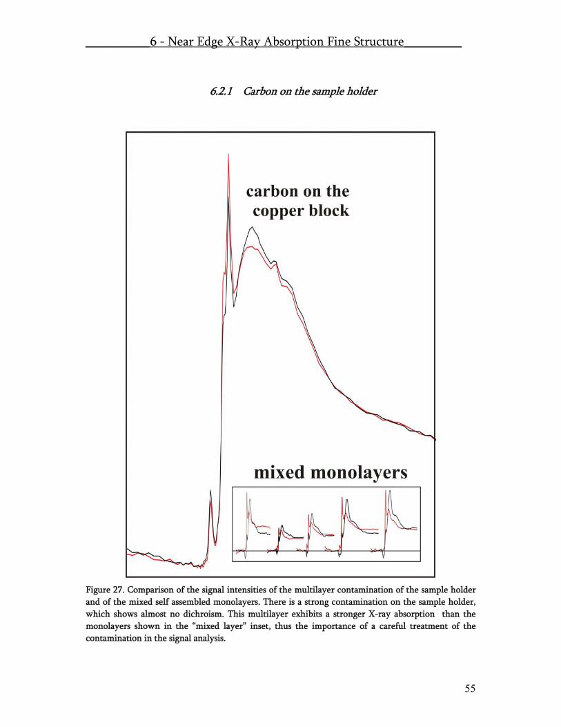
__________6 - Near Edge X-Ray Absorption Fine Structure_________
55
6.2.1 Carbon on the sample holder
Figure 27. Comparison of the signal intensities of the multilayer contamination of the sample holder and of the mixed self assembled monolayers. There is a strong contamination on the sample holder, which shows almost no dichroism. This multilayer exhibits a stronger X-ray absorption than the monolayers shown in the “mixed layer” inset, thus the importance of a careful treatment of the contamination in the signal analysis.

__________6 - Near Edge X-Ray Absorption Fine Structure_________
56
In the inset of Figure 24. one can see the samples (the gold shining pieces) used to measure the data which is presented in Figure 27 as “mixed monolayers” (which are thoroughly discussed in the publication “Co-assembly – concentration and mixing dependent ordering”). In the same measurement series we determined the carbon contamination on the copper plate (also visible on the inset in Figure 5) underneath the SAM samples. et the big NEXAFS spectra of Figure 27. The relative signal intensities comparing the monolayers and the “copper-carbon” show that there is a non-oriented multilayer containing some, rather little abundance of aromatic compounds.
6.2.2 Orientation of BDMT on Au(111)
Figure 28. The polarisation dependence of NEXAFS spectra of a BDMT SAM on Au(111). The clear dichroism of the peak at 285 eV shows that the molecules are oriented on the surface, the phenyl ring plane standing close to perpendicular with respect to the surface plane.
__________6 - Near Edge X-Ray Absorption Fine Structure_________
57
In Figure 28 we show a series of polarisation dependent measurements (90°, 45° and 0°) of a BDMT SAM. The data was acquired and analysed in the same experimental run as in the one shown in Figure 7. One can clearly see a strong polarisation dependence. The main features in the NEXAFS signal correspond to the phenyl ring. The assigned π*1, π*2 and σ*1 and σ*2 can be qualitatively interpreted by comparison to the characterisation of the phenyl system in Figure 3. If the polarisation of the incoming x-ray is perpendicular to the phenyl ring the absorption signal of the π* resonances is maximal and for the σ* resonances it is the opposite. Thus it concludes from this data that BDMT forms oriented layers on Au(111). Another, interesting detail is visible in the inset of Figure 8. The small absorption peak at 286.6 eV has previously been attributed to the C-S* resonance87. In the case of the mercaptobenzene this feature is dependent on the direction of the benzene ring (in the same plane). In our study, in the case of BDMT the C-S bond can freely rotate and shows a different dependence on the polarisation than the benzene ring. The obtained NEXAFS results and the appropriate discussion on it can be found in the publication chapter of this thesis (see “Co-assembly – concentration and mixing dependent binary SAM structures” and “Gel-assisted host/guest assembly of dithiocarbamates and thiols”).
87 Stöhr, J. and Outka, D.A. Phys. Rev. B 36 (1987) 7891.

58
59
7 Collected Publications Dithiocarbamates: functional and versatile linkers for the formation of self-assembled monolayers. & Supporting Information Supramolecular surface assembly of dithiocarbamates on Au(111): Chiral trimeric domains and amorphous structures. & Supporting Information. Co-assembly – concentration and mixing dependent binary SAM structures: Mechanisms of molecular 2D ordering investigated by NEXAFS and STM. & Supporting Information. Gel-assisted host/guest assembly of dithiocarbamates and thiols: Analysis of local orientation and conductivity within ternary assemblies. & Supporting Information.


61
8 Dithiocarbamates: functional and versatile linkers for the formation of self-assembled monolayers.
Peter Morf*, Fabio Raimondi†, Heinz-Georg Nothofer‡, Bernhard Schnyder†, Akio
Yasuda‡, Jurina M. Wessels‡ and Thomas A. Jung*
*Laboratory for Micro and Nanotechnology, Paul Scherrer Institut, 52 Villigen
Switzerland.
†Laboratory for Electrochemistry, Paul Scherrer Institut, 5232 Villigen Switzerland.
‡Sony Deutschland GmbH, Stuttgart Technology Center, Materials Science Laboratory,
Hedelfingerstrasse 61, D-70327 Stuttgart.
Abstract:
Self-assembled monolayers have evolved into one of the best established self-assembly systems with high relevance in a scientific and applied context1-4. So far, however, virtually exclusively thiol functional groups have been used for the investigation of fundamental processes on metal surfaces. In this paper, an alternative binding group, the dithiocarbamate (DTC) group is re-visited: Complete SAM formation with new layer properties characteristically different from thiol SAMs is demonstrated for mono-functional acyclic and bifunctional cyclic dithiocarbamates on Au(111) by X-ray photoelectron spectroscopy, cyclic voltammetry and scanning tunneling microscopy. Furthermore, the chemical
___8 - Dithiocarbamates: functional and versatile linkers for SAMs___
62
adsorption and voltammetric desorption reactions are quantitatively determined. The resonant bi-dentate structure of the DTC provides a characteristically different molecule-metal coupling compared to the thiols and makes the DTC an interesting system for molecular electronics.
1. Introduction
The general concept of self assembled monolayer (SAM) formation involves the selective binding of molecules to a flat surface followed by periodic rearrangement, driven by thermal motion and intermolecular forces. Ever since the first reports about the binding of thiols to platinum5 and the adsorption and SAM formation of alkyl disulfide6, thiophene derivatives7,8 and alkanethiols9 on flat gold surfaces, an overwhelming variety of thiol functionalised molecules has been used to explore fundamental processes at interfaces1-3,10. For alkanethiols extended 2D patterns1,11 were observed after assembly over days and weeks. Also compounds like thiolates12, xanthates13 and dithiocarbamates have been investigated earlier14,15. The dithiocarbamate (DTC) binding group differs much from the thiol binding group. In particular the entire N-C-S2 group forms a resonant structure16. This leads to characteristically different physical and chemical properties e.g. the striking optical and electronical behaviour described for DTC derivatives when interlinking nanoparticles17. The general chemistry of DTC derivatives is well known16, and thermal stability18 as well as decomposition under acidic conditions has been studied in detail19,20.
In this study DTCs have been investigated with the particular focus on the binding characteristics and SAM formation of mono-functional acyclic and bifunctional cyclic DTC derivatives on flat Au(111) surfaces. X-ray photoelectron spectroscopy (XPS), cyclic voltammetry (CV) and scanning tunnelling microscopy (STM) provide clear evidence for layer formation and the binding of the resonant DTC group to the Au(111) surface.
2. Materials and Methods Materials Ethanol, DMF (crown capped), DMSO and KOH were used as provided by Fluka
in p.a. quality. Water was purified using a MilliQ-system (Millipore Biocel). Octanethiol (OT) (>98.5%) and 1,4-bis(mercaptomethyl)benzene (BDMT) (98%), tetramethylthiuram disulfide (thiram) (99%) and sodium N,N-diethyldithiocarbamate·3H2O (DEDT) (>99%) were obtained from Sigma-Aldrich

___8 - Dithiocarbamates: functional and versatile linkers for SAMs___
63
and used without further purification. The 1,4-cyclohexane-bis-(dithiocarbamate) sodium salt (cHBDT) and 1,4-phenylene-bis-(dithiocarbamate) sodium salt (PBDT) were synthesised at the Sony Materials Science Laboratory17.
Au(111) film preparation Epitaxial Au(111) films exhibiting extended terraces were produced by
sublimation of 120-150 nm gold onto freshly cleaved mica samples held at 340 °C. Subsequently the Au film was heated up to 540 °C for 5-10 min. and was allowed to cool down in two steps: 5 min. at 500 °C, 5 min. at 450 °C before re-equilibration to room temperature. This annealing procedure reproducibly leads to uniform surfaces exhibiting characteristic triangular terraces in (111) orientation and typically 200 x 200 nm2 in size.
SAM preparation All SAM layers were assembled onto the Au(111) substrate by exposure to
solutions. Solvents and concentrations were chosen in dependence of the solubility of the compounds. For octanethiol, 1mM in ethanol; for BDMT, 0.2 mM in toluene or DMF; for thiram, 1 mM in 1/1 ethanol/DMF; for DEDT, 1mM in ethanol; for PBDT and cHBDT, 1 mM in 1/1 ethanol (or DMF)/0.5% aqueous NaOH were chosen. The SAM layers of PBDT and cHBDT were assembled from ethanolic alkaline solution in order to prevent the decomposition which has been described in earlier studies19,20. For all investigations the same assembly procedures were applied to equally prepared substrates.
XPS-experiments The XP-spectra were recorded with an ESCALAB 220i XL (VG Scientific)
photoelectron spectrometer. Mg and Al Kα-radiation was used to investigate the bulk-like thick film or powder samples whereas monochromatic Al Kα-radiation (1486.6 eV) was used to obtain the XP spectra of SAM layers. The spectra were recorded in constant analyser energy (CAE) mode with analyser path energies of 50 eV for the survey spectra and 20 eV for high-resolution spectra.
Direct comparison of the measured XPS binding energies between the powder and the monolayer sample is not accurate, because of differences in the charging of the powder samples and the presence of carbon contaminants on the monolayer. Thus, the relative calibration of the measured spectra depends on the choice of the reference atomic systems21. The powder spectra of the acyclic molecules were calibrated using the N 1s binding energy (400.00 eV) while for the cyclic molecule the Na 1s binding energy (1072.99 eV) was used. The binding energies of the SAM

___8 - Dithiocarbamates: functional and versatile linkers for SAMs___
64
samples were interpreted without a relative compensation of the energy scale. This is justified by the insignificant charging of a single molecular layer compared to the powder samples.
CV-experiments Electrochemical experiments were performed using a BAS 100a Electrochemical
Analyser with a home built electrochemical cell. As reference electrode a Hg+/HgO [OH-] system was chosen. Freshly evaporated Au(111) films on mica were punched into identical round pieces (Ø 8mm) to be mounted on a dedicated, gold plated clamp after preparation. All electrochemical experiments were performed in de-aerated 0.5M KOH in aqueous solution.
STM-experiments STM experiments were performed using a Nanoscope III Multimode low current
STM and Omicron UHV-AFM/STM. Tunnelling current and bias potential were kept at 2 pA and 100 mV for the imaging of all SAMs. UHV-STM experiments at 70 pA and 500 mV were performed on DEDT SAMs for comparison. Pt/Ir (80/20) tips were cut from 0.25mm diam. wire for all experiments.
3. Research design Chemical binding to Au(111) substrates and self-assembled monolayer formation
of the acyclic and cyclic DTC derivatives, thiram, DEDT, PBDT and cHBDT, were compared to the corresponding properties of the acyclic octanethiol OT and the cyclic dithiol BDMT. The Au-sulfur interaction and the total amount of sulfur abundant on the surface was analysed using XPS22,23. For this purpose, the sulfur 2p XPS signal of each species is identified by the two sharp 2p1/2 and 2p3/2 peaks split by the spin-orbit coupling. The peaks are showing a relative ratio of 1:2 and are separated by 1.18 eV24. The 2p3/2 binding energy is referred to as the 2p binding energy and is determined by the net charging25,26 of the investigated species22. This is typically referred to as the ‘chemical shift’ of the studied species.
Cyclic voltammograms have been recorded in order to explore the electrochemical binding characteristics of DTCs and thiols to Au(111) substrates: In consecutive experimental cycles, peaks corresponding to the desorption and re-adsorption process are identified. Quantitative analysis of the first CV cycle provides a measure for the number of charges involved in the reductive desorption process of the studied SAM. In combination, XPS and CV reveal the stoichiometry of the electrochemical desorption. The observed decline of the reductive desorption peak

___8 - Dithiocarbamates: functional and versatile linkers for SAMs___
65
corresponds to the incomplete re-adsorption of an accountable fraction of the originally assembled layer.
Furthermore the layer and substrate morphology of thermally well equilibrated samples was analysed in detail by STM, which had been established early on for the structural study of thiol SAMs27-33. All displayed data are a representative selection from a larger set, which has been taken from at least 2 experiments reproduced under identical conditions (XPS: 2-5, CV: 4-10, STM: 3-4 experimental runs).
4. Results and Discussion 1. Monofunctional acyclic molecules Figure 8.1a shows the XPS spectrum of a thiram powder sample and a SAM formed
from thiram on Au(111). The powder spectrum of thiram shows two S-species, one at 161.6 eV corresponding to the C=S entity and one at 163.6 eV corresponding to the disulfide. This is in in very good agreement with the early and detailed assessment of sulfur compounds by Lindberg et al. reporting a binding energy of 161.8 and 163.8 eV for the thiram sulfur species25. In contrast, the XPS spectrum of a SAM formed from thiram on Au(111) shows only one sulfur species at 161.8 eV. This result provides clear evidence for the reactive chemisorption of thiram in a certain analogy to the well-discussed disulfide case1,6,10,34. The disulfide bridge in thiram cleaves at the Au surface, leading to a bidentate state where both sulfur atoms of the dimethyldithiocarbamates (DMDT) bind symmetrically to the surface. This is in agreement with a previous assessment of thiram adsorption on rough gold35 and on rough silver surfaces36on the basis of FT-IR and surface enhanced Raman spectroscopy (SERS). Figure 8.1b shows the XPS spectrum of the powder and SAM on Au(111) of DEDT – a dithiocarbamate sodium salt. The sodium ions are fully exchanged upon chemisorption of DEDT onto gold. Less than 1% sodium of the stoichiometric ratio to sulfur was detected in XPS. The S 2p binding energy of the bidentate state in the powder and the SAM is equal (161.6 eV) and comparable with the binding energy of DMDT on Au. It is further pertinent to note that there is a small but distinct change in the difference of the N1s and the S2p binding energies (Δ(N,S)), which is a measure of the electron distribution on the resonant DTC-entity that has been previously detected via the C=N double bond characteristic in FT-IR studies of DTC salts15, surface assemblies35 and DTC linked to Au-colloids37. For the DEDT powder sample Δ(N,S) amounts to 238.36±0.01 eV. Upon adsorption to Au(111) this value decreases to 238.02±0.01 eV. DMDT SAMs exhibit the same Δ(N,S) value, 238.05±0.08 eV. This result provides evidence for the DTC-entity in both the DEDT and DMDT layers exhibiting the same electronic configuration.
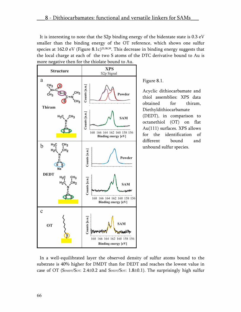
___8 - Dithiocarbamates: functional and versatile linkers for SAMs___
66
It is interesting to note that the S2p binding energy of the bidentate state is 0.3 eV smaller than the binding energy of the OT reference, which shows one sulfur species at 162.0 eV (Figure 8.1c)23,38,39. This decrease in binding energy suggests that the local charge at each of the two S atoms of the DTC derivative bound to Au is more negative then for the thiolate bound to Au.
In a well-equilibrated layer the observed density of sulfur atoms bound to the
substrate is 40% higher for DMDT than for DEDT and reaches the lowest value in case of OT (SDMDT/SOT: 2.4±0.2 and SDEDT/SOT: 1.8±0.1). The surprisingly high sulfur
Figure 8.1.
Acyclic dithiocarbamate and thiol assemblies: XPS data obtained for thiram, Diethyldithiocarbamate (DEDT), in comparison to octanethiol (OT) on flat Au(111) surfaces. XPS allows for the identification of different bound and unbound sulfur species.

___8 - Dithiocarbamates: functional and versatile linkers for SAMs___
67
density of the DTC films is constant for equally prepared substrates and suggests the formation of compact molecular layers. Decomposition on the surface can be excluded on the basis of the S/N ratio measured by XPS (stoichiometry: 2/1; DMDT: 1.9±0.5; DEDT: 1.9±0.5). The difference in the S density between the DMDT and the DEDT SAMs can qualitatively be explained by steric constraints of the ethyl and the methyl chain in the molecular backbone (see Supporting Information, Figure 8.7). In case of a densely packed OT SAM, the spatial separation of the S atoms is determined by the S-Au interaction. In case of the DTCs however, the resonant structure of the binding group seems to open up the possibility of packing, which is determined by the interaction of the molecular backbone, since the N-C-S2 entity is energetically degenerate with respect to the binding site.
Through reductive desorption in cyclic voltammetry (CV) we verify the binding properties of thiuram disulfides and dithiocarbamates to Au(111)40 in analogy to a previous study on xanthates41. For DMDT, DEDT and OT SAMs a characteristic desorption and re-adsorption behavior is observed: The first, reductive sweep is characterized by a pronounced desorption peak at a characteristic potential, which is similar in potential for DMDT (-791±18 mV vs. Hg/HgO [OH-]) and DEDT (-759±8 mV vs. Hg/HgO [OH-]) but distinctively more positive compared to the OT SAM reference (Figure 8.2). When sweeping back in potential, a small re-adsorption peak occurs. This is related to the fraction of molecules that did not diffuse into the solution and are re-adsorbing on the electrode. Consequently, a second reductive sweep shows a lower desorption peak: a behaviour which is well known from the alkanethiol systems12 and provides complementary evidence for SAM formation from thiram and DEDT.
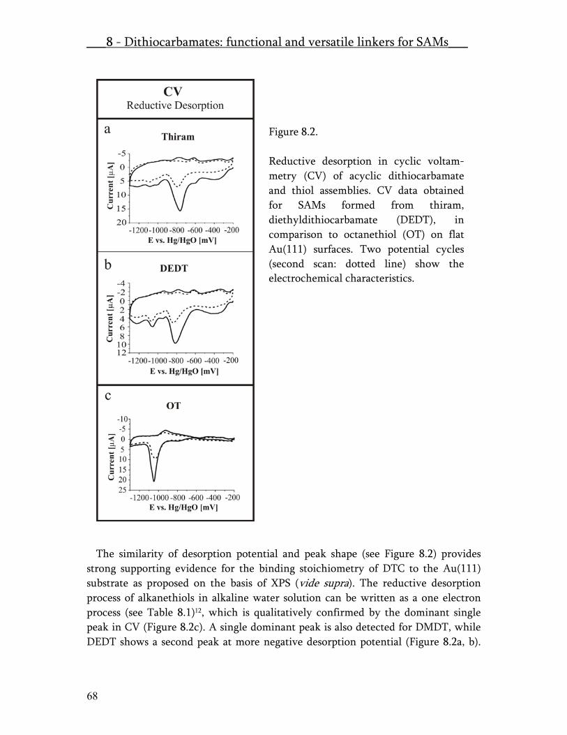
___8 - Dithiocarbamates: functional and versatile linkers for SAMs___
68
The similarity of desorption potential and peak shape (see Figure 8.2) provides strong supporting evidence for the binding stoichiometry of DTC to the Au(111) substrate as proposed on the basis of XPS (vide supra). The reductive desorption process of alkanethiols in alkaline water solution can be written as a one electron process (see Table 8.1)12, which is qualitatively confirmed by the dominant single peak in CV (Figure 8.2c). A single dominant peak is also detected for DMDT, while DEDT shows a second peak at more negative desorption potential (Figure 8.2a, b).
Figure 8.2. Reductive desorption in cyclic voltam-metry (CV) of acyclic dithiocarbamate and thiol assemblies. CV data obtained for SAMs formed from thiram, diethyldithiocarbamate (DEDT), in comparison to octanethiol (OT) on flat Au(111) surfaces. Two potential cycles (second scan: dotted line) show the electrochemical characteristics.

___8 - Dithiocarbamates: functional and versatile linkers for SAMs___
69
The second small peak may be caused by molecules that are adsorbed at different binding sites or show a different packing on the Au(111) surface. In order to determine the number of electrons involved in the reactive adsorption and desorption process, the absolute sulfur density of the DMDT and DEDT SAM was analysed by XPS relative to a densely packed OT SAM. The charge per surface area was determined by integration of the CV desorption peaks. The resulting ratio of electrons per bound sulfur atom was determined to be 0.44±0.09 e-/sulfur atom for DEDT and 0.45±0.05 e-/sulfur atom for DMDT, respectively. Thus the adsorption/desorption process for dithiocarbamate and thiuram disulfides to/from Au(111) surfaces can be written as displayed in Table 8.1. Table 8.1. Chemisorption and reductive desorption reactions of different sulfur compounds at the Au(111) surface.
Adsorption on Au(111) Desorption from Au(111)
Thiuram disulfides R2NC(S)S-S(S)CNR2 + 2 Au(0)
2 AuS2CNR2
AuS2CNR2 + e-
Au(0) + -S2CNR2
Dithiocarbamates NaS2CNR2 + Au(0)
Na+ + [AuS2CNR2]-
AuS2CNR2 + e-
Au(0) + -S2CNR2
Thiols R-SH + Au(0)
AuS-R + ½H2
AuS-R + e-
Au(0) + -S-R
Disulfides R-S-S-R + 2Au(0)
2AuS-R
AuS-R + e-
Au(0) + -S-R
Thiolates R-SNa + Au(0)
[AuS-R]- + Na+
AuS-R + e-
Au(0) + -S-R
Complementary STM experiments clearly showed distinct differences between
DTC SAMs and thiolate SAMs. In Figure 8.3a, the latter reference system reproduced the distinct ( 3 × 3 )R30° and (2 3 ×3)R30° superstructure42 and etch pits as they are well known from earlier studies31-33. The dithiocarbamate derivatives,
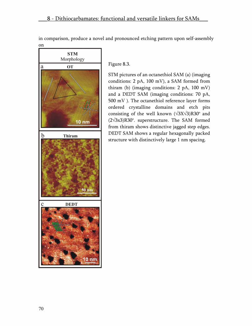
___8 - Dithiocarbamates: functional and versatile linkers for SAMs___
70
in comparison, produce a novel and pronounced etching pattern upon self-assembly on
Figure 8.3.
STM pictures of an octanethiol SAM (a) (imaging conditions: 2 pA, 100 mV), a SAM formed from thiram (b) (imaging conditions: 2 pA, 100 mV) and a DEDT SAM (imaging conditions: 70 pA, 500 mV ). The octanethiol reference layer forms ordered crystalline domains and etch pits consisting of the well known (√3X√3)R30° and (2√3x3)R30°. superstructure. The SAM formed from thiram shows distinctive jagged step edges. DEDT SAM shows a regular hexagonally packed structure with distinctively large 1 nm spacing.
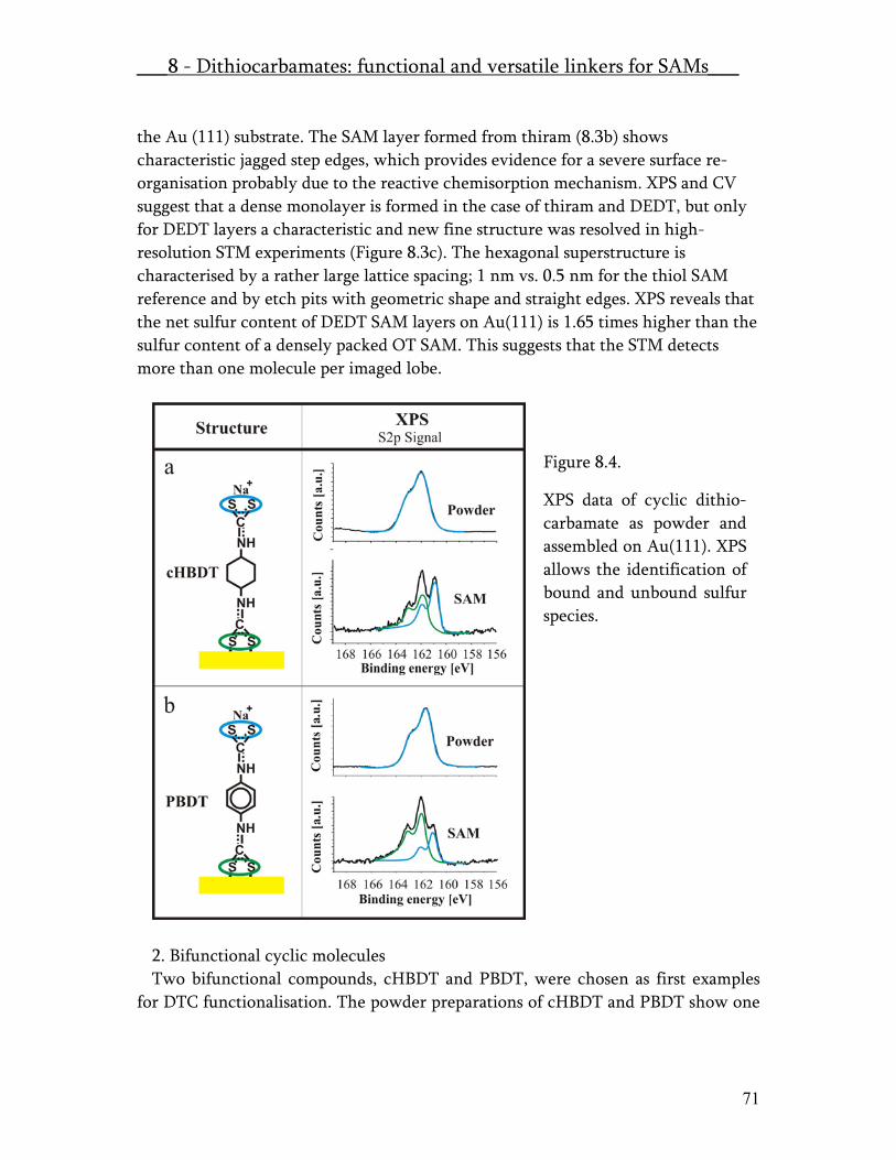
___8 - Dithiocarbamates: functional and versatile linkers for SAMs___
71
the Au (111) substrate. The SAM layer formed from thiram (8.3b) shows characteristic jagged step edges, which provides evidence for a severe surface re-organisation probably due to the reactive chemisorption mechanism. XPS and CV suggest that a dense monolayer is formed in the case of thiram and DEDT, but only for DEDT layers a characteristic and new fine structure was resolved in high-resolution STM experiments (Figure 8.3c). The hexagonal superstructure is characterised by a rather large lattice spacing; 1 nm vs. 0.5 nm for the thiol SAM reference and by etch pits with geometric shape and straight edges. XPS reveals that the net sulfur content of DEDT SAM layers on Au(111) is 1.65 times higher than the sulfur content of a densely packed OT SAM. This suggests that the STM detects more than one molecule per imaged lobe.
2. Bifunctional cyclic molecules Two bifunctional compounds, cHBDT and PBDT, were chosen as first examples
for DTC functionalisation. The powder preparations of cHBDT and PBDT show one
Figure 8.4.
XPS data of cyclic dithio-carbamate as powder and assembled on Au(111). XPSallows the identification of bound and unbound sulfur species.

___8 - Dithiocarbamates: functional and versatile linkers for SAMs___
72
sulfur peak at a binding energy of 161.9 and 161.7 eV, respectively. After SAM formation, two sulphur signals can be detected for both compounds at 161.0 eV and at 162.0 eV (see Figure 8.4a, b). This suggests that both molecules chemisorb to the Au(111) substrate with one DTC end group, while the other DTC end group remains bound to the sodium ion. A significant decomposition of the compounds can be ruled out, since both spectra showed that more than 92% of the sulfur is either bound to Au or complexed with Na. Based on the quantification of the occurring sulfur species in comparison to the abundance of the sodium counter ion of the free DTC group, we identify S-Au with the binding energy at 162.0 eV and S-Na with the binding energy of 161.0 eV (see Supporting Information for detailed discussion). The binding energy of the S2p electrons from the bifunctional molecules is ~0.3 eV higher than that of the monofunctional DEDT and DMDT molecules, indicating differences in the electronic structure of the DTC binding group of both systems. Further analysis revealed that the density of bound sulfur species is 80% higher for PBDT than for cHBDT (SPBDT/SOT : 1.9±0.1 and ScHBDT/SOT : 1.1±0.1). One possible explanation is that the π- π-interaction of the benzene moiety in PBDT leads to a denser packing on the Au surface. Another possibility is that the degree of order and orientation of both molecules in the SAM differs. Some molecules may be lying flat, possibly even bound with both ends to the Au surface, while others are bound to Au with one end. Such independent layering could also explain the inequivalent peak intensities of the two S species in the XP spectra (S-Au/S-Na of cHBDT: 1.0±0.1 and PBDT 3.4±0.7). However, we would like to point out that these differences can also be related to the scattering of photoelectrons. It is important to note that the peak shape of the N1s signal from the cHBDT and PBDT SAM is significantly broadened compared to DMDT and DEDT (Supporting Information, Figure 8.7a and b). This indicates that the electron density on the two nitrogen species (associated with the DTC-Au or DTC-Na group) in the cHBDT and PBDT SAMs differs due to alteration in the charge that is transferred from either Au to DTC or Na to DTC. In this context we would like to point out, that the charge transfer from Au to thiols and DTC differs, which is apparent in the small but reproducible shift (measured over a 1 ½ y period) in the Au(4f7/2) electron binding energy of thiol SAMs (83.88±0.03eV) and dithiocarbamate SAMs (83.69±0.09eV). The thiol group exhibits an increased oxidative strength on Au(111) compared to the dithiocarbamate group (Supporting Information, Figure 8.10).
CV experiments with the bisdithiocarbamate derivatives show characteristic
desorption peaks at a potential that is significantly more negative than in the case of DEDT and DMDT, i.e. -1012±6 mV and -1023±12 mV vs. Hg/HgO [OH-]. Thus dithiocarbamates follow the same trend as it is well established for thiols: the longer
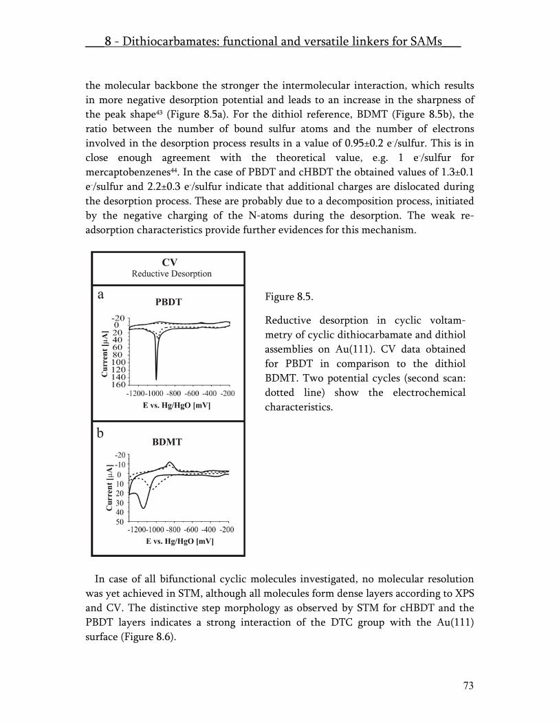
___8 - Dithiocarbamates: functional and versatile linkers for SAMs___
73
the molecular backbone the stronger the intermolecular interaction, which results in more negative desorption potential and leads to an increase in the sharpness of the peak shape43 (Figure 8.5a). For the dithiol reference, BDMT (Figure 8.5b), the ratio between the number of bound sulfur atoms and the number of electrons involved in the desorption process results in a value of 0.95±0.2 e-/sulfur. This is in close enough agreement with the theoretical value, e.g. 1 e-/sulfur for mercaptobenzenes44. In the case of PBDT and cHBDT the obtained values of 1.3±0.1 e-/sulfur and 2.2±0.3 e-/sulfur indicate that additional charges are dislocated during the desorption process. These are probably due to a decomposition process, initiated by the negative charging of the N-atoms during the desorption. The weak re-adsorption characteristics provide further evidences for this mechanism.
In case of all bifunctional cyclic molecules investigated, no molecular resolution
was yet achieved in STM, although all molecules form dense layers according to XPS and CV. The distinctive step morphology as observed by STM for cHBDT and the PBDT layers indicates a strong interaction of the DTC group with the Au(111) surface (Figure 8.6).
Figure 8.5.
Reductive desorption in cyclic voltam-metry of cyclic dithiocarbamate and dithiol assemblies on Au(111). CV data obtained for PBDT in comparison to the dithiol BDMT. Two potential cycles (second scan: dotted line) show the electrochemical characteristics.
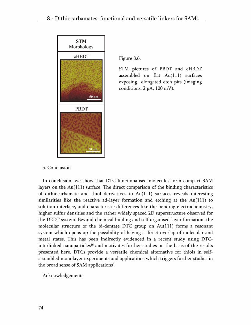
___8 - Dithiocarbamates: functional and versatile linkers for SAMs___
74
5. Conclusion In conclusion, we show that DTC functionalised molecules form compact SAM
layers on the Au(111) surface. The direct comparison of the binding characteristics of dithiocarbamate and thiol derivatives to Au(111) surfaces reveals interesting similarities like the reactive ad-layer formation and etching at the Au(111) to solution interface, and characteristic differences like the bonding electrochemistry, higher sulfur densities and the rather widely spaced 2D superstructure observed for the DEDT system. Beyond chemical binding and self organised layer formation, the molecular structure of the bi-dentate DTC group on Au(111) forms a resonant system which opens up the possibility of having a direct overlap of molecular and metal states. This has been indirectly evidenced in a recent study using DTC-interlinked nanoparticles16 and motivates further studies on the basis of the results presented here. DTCs provide a versatile chemical alternative for thiols in self-assembled monolayer experiments and applications which triggers further studies in the broad sense of SAM applications5.
Acknowledgements
Figure 8.6.
STM pictures of PBDT and cHBDT assembled on flat Au(111) surfaces exposing elongated etch pits (imaging conditions: 2 pA, 100 mV).

___8 - Dithiocarbamates: functional and versatile linkers for SAMs___
75
This work was financially supported by Sony Deutschland GmbH – Materials Science Laboratory. T.J. acknowledges financial contributions from the Swiss National Science Foundation and the NCCR Nanosciences. It is a pleasure to acknowledge interesting and helpful discussions with Ch. Schoenenberger and Florian von Wrochem. Beat Steiger and Celestino Padeste are thanked for sharing their expertise in electrochemistry. PSI’s analytical services are acknowledged for providing AES data. In particular J. Wimmer is thanked for the IR and SERS as well as J. J. Hefti for his assistance with CV.
Supporting Information Available:
The N1s XPS-signals of thiram, DEDT, cHBDT and PBDT SAMs, gold 4f 7/2 XPS-binding energies for thiol and DTC SAMs and space-filling models. This material is available free of charge via the Internet at http://pubs.acs.org.
______________________________________________________________________ 1 Ulman, A. An Introduction to Ultrathin Organic Films, Academic Press, Boston, 1991.
2 Ed. Ulman, A. Thin Films, Volume 20, Organic Thin Films and Surfaces, Academic Press, Boston, 1995.
3 Ed. Ulman A. Thin Films, Volume 24, Self-Assembled Monolayers of Thiols, Academic Press, Boston 1998.
4 Love, J.C.; Estroff, L.A.; Kriebel, J.K.; Nuzzo, R.G. and Whitesides, G.M. Chem. Rev. 105 (2005) 1103.
5 Mexted, E.B. Advan. Catal. 3 (1951) 129.
6 Nuzzo, R.G.; Allara, D.L. J. Am. Chem. Soc. 105 (1983) 4481.
7 Li, T.T-T.; Liu, H.Y. and Weaver, M.J. J. Am. Chem. Soc. 106 (1984) 1233.
8 Li, T.T-T. and Weaver, M.J. J. Am. Chem. Soc. 106 (1984) 6107.
9 Strong, L. and Whitesides, G.M. Langmuir 4 (1988) 546.
10 Schreiber, F. Prog. Surf. Sci. 65 (2000) 151.
11 Badia, A.; Back, R. and Lennox, R.B. Angew. Chem. Int. Ed. Engl. 33 (1994) 2332.
12 Widrig, C.A.; Chung, C. and Porter M.D. J. Electroanal. Chem. 310 (1991) 335.

___8 - Dithiocarbamates: functional and versatile linkers for SAMs___
76
13 Ihs, A.; Uvdal, K. and Liedberg, B. Langmuir 9 (1993) 733.
14 Footnote 30 in Bain, C.D.; Evall, J. and Whitesides, G.M. J. Am. Chem. Soc. 111 (1989) 7155.
15 Arndt, Th.; Schupp, H. and Schrepp, W. Thin Solid Films 178 (1989) 319.
16 Thorn, G.D. and Ludwig, R.A. The Dithiocarbamates and Related Compounds, Elsevier, Amsterdam – New York 1962.
17 Wessels, J.M.; Nothofer. H-G.; Ford, W.E.; von Wrochem, F.; Scholz, F.; Vossmeyer, T.; Schroedter, A.; Weller, H.; Yasuda, Akio. J. Am. Chem. Soc. 126 (2004) 3349.
18 Hill, J.O. and Magee, R.J. Rev. Inorg. Chem. 3 (1981) 141.
19 Ewing, S.P.; Lockshon, D. and Jencks, W.P. J. Am. Chem. Soc. 102 (1980) 3072.
20 Humeres, E.; Debacher, N.A.; de S. Sierra, M.M.; Franco, J.D. and Schutz, A. J. Org. Chem. 63 (1998) 1598.
21 Beamson, G. and Briggs, D. High Resolution XPS on Organic Polymers, John Wiley & Sons Ltd. Chichester, 1992.
22 Briggs, D. and Seah, M.P. Practical Surface Analysis, second edition, Volume 1, John Wiley & Sons, Chichester, 1990.
23 Duvez A-S. J. Electron Spectrosc. Relat. Phenom. 134 (2004) 97.
24 Handbook of X-Ray Photoelectron Spectroscopy, Perkin-Elmer Corporation, 1992.
25 Lindberg, B.J.; Hamrin, K.; Johansson, G.; Gelius, U.; Fahlman, A.; Nordling, C. and Siegbahn K. Phys. Scr. 1 (1970) 286.
26 Hamrin, K.; Johansson, G.; Fahlman, A.; Nordling, C.; Siegbahn, K. and Lindberg, B. Chem. Phys. Lett. 1 (1967) 557.
27 Widrig, C.A.; Alves, C.A. and Porter, M.D. J. Am. Chem. Soc. 113 (1991) 2805.
28 Kim, Y-T. McCarley, R.L. and Bard, A.J. J. Phys. Chem. 96 (1992) 7416.
29 Poirier, G.E. and Tarlov, M.J. Langmuir 10 (1994) 2853.
30 Schönenberger, C.; Jorritsma, J.; Sondag-Huethorst, J.A.M. and Fokkink, L.G.J. J. Phys. Chem. 99 (1995) 3259.

___8 - Dithiocarbamates: functional and versatile linkers for SAMs___
77
31 Kim, Y-T. and Bard, A.J. Langmuir 8 (1992) 1096.
32 Schönenberger, C.; Sondag-Huethorst, J.A.M.; Jorritsma, J. and Fokkink, L.G.J. Langmuir 10 (1994) 611.
33 Häussling, L.; Michel, B.; Ringsdorf, H. and Rohrer, H. Angew. Chem. Int. Ed. Engl. 30 (1991) 569.
34 Nuzzo, R.G. ; Fusco, F.A. and Allara, D.L. J. Am. Chem. Soc. 109 (1987) 2358.
35 Sánchez-Cortés, S.; Domingo, C. ; García-Ramos, J.V. ; Aznárez, J.A. Langmuir 17 (2001) 1157.
36 Kang, J.S.; Hwang, S.Y.; Lee, C.J. and Lee, M.S. Bull. Korean. Chem. Soc. 23 (2002) 1604.
37 Zhao, Y.; Pérez-Segarra, W.; Shi, Q. and Wei, A. J. Am. Chem. Soc. 127 (2005) 7328.
38 Bain C.D., Biebuyck H.A., Whitesides G.M. Langmuir 5 (1989) 723.
39 Nuzzo, R.G.; Zegarski B.R.; Dubois, L.H. J. Am. Chem. Soc. 109 (1987) 733.
40 Procopio, J.R.; Escribano, M.T.S. and Hernandez, L.H. Fresenius Z. Anal. Chem. 311 (1988) 27.
41 Gothelf, K.V. J. Electroanal. Chem. 494 (2000) 147.
42 Poirier, G.E. and Tarlov, M.J. Langmuir 10 (1994) 2853.
43 Kakiuchi, T.; Usui, H.; Hobara, D. and Yamamoto, M. Langmuir 18 (2002) 5231.
44 Batz, V.; Schneeweiss, M.A.; Kramer, D.; Hagenström, H.; Kolb, D.M. and Mandler, D. J. Electroanal. Chem. 491 (2000) 55.
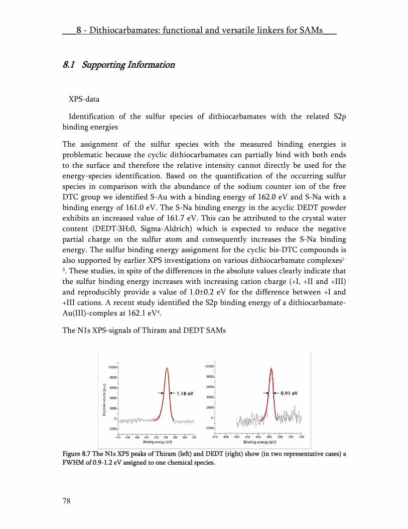
___8 - Dithiocarbamates: functional and versatile linkers for SAMs___
78
8.1 Supporting Information
XPS-data
Identification of the sulfur species of dithiocarbamates with the related S2p binding energies
The assignment of the sulfur species with the measured binding energies is problematic because the cyclic dithiocarbamates can partially bind with both ends to the surface and therefore the relative intensity cannot directly be used for the energy-species identification. Based on the quantification of the occurring sulfur species in comparison with the abundance of the sodium counter ion of the free DTC group we identified S-Au with a binding energy of 162.0 eV and S-Na with a binding energy of 161.0 eV. The S-Na binding energy in the acyclic DEDT powder exhibits an increased value of 161.7 eV. This can be attributed to the crystal water content (DEDT·3H20, Sigma-Aldrich) which is expected to reduce the negative partial charge on the sulfur atom and consequently increases the S-Na binding energy. The sulfur binding energy assignment for the cyclic bis-DTC compounds is also supported by earlier XPS investigations on various dithiocarbamate complexes1-
3. These studies, in spite of the differences in the absolute values clearly indicate that the sulfur binding energy increases with increasing cation charge (+I, +II and +III) and reproducibly provide a value of 1.0±0.2 eV for the difference between +I and +III cations. A recent study identified the S2p binding energy of a dithiocarbamate-Au(III)-complex at 162.1 eV4.
The N1s XPS-signals of Thiram and DEDT SAMs
Figure 8.7 The N1s XPS peaks of Thiram (left) and DEDT (right) show (in two representative cases) a FWHM of 0.9-1.2 eV assigned to one chemical species.

___8 - Dithiocarbamates: functional and versatile linkers for SAMs___
79
The N1s XPS-signal of cHBDT and PBDT SAMs
Figure 8.8 The N1s XPS peaks of PBDT (left) and cHBDT (right) are much broader (FWHM: 1.8-2.0 eV ) compared to the signals in Figure 8.7, which evidences the existence of two nitrogen species.
The broadening of the N1s can be explained by the presence of two nitrogens
resulting after adsorption of the cyclic molecules:
Figure 8.9 Thiram and DEDT (left) are showing only one nitrogen species as SAM and as powder, whereas the cHBDT and PBDT (right) as SAM are bearing two chemically differing nitrogens.
Gold 4f 7/2 binding energies for thiol and DTC SAMs

___8 - Dithiocarbamates: functional and versatile linkers for SAMs___
80
Figure 8.10 shows the gold 4f 7/2 electron binding energies for all investigated thiol and DTC SAMs. There is small but distinct difference between the thiol (OT: 83.90 eV, DT: 83.85 eV and BDMT: 83.90 eV) and DTC (Thiram: 83.60 eV, DEDT: 83.60 eV, cHBDT: 83.70 eV and PBDT: 83.75 eV) compounds. The data were taken over a time periode larger than one year. This indicates that instrumental fluctuations can be ruled out to explain these differences.
Space filling Models
Figure 8.11 Dimethyldithocarbamate (disotiated Thiram) and DEDT (without sodium cation). The diethyl chains of DEDT (right) are resulting in a much “bulkier” structure than the dissociated Thiram entity. Thiram SAMs show 40% higher sulfur density as measured for DEDT.
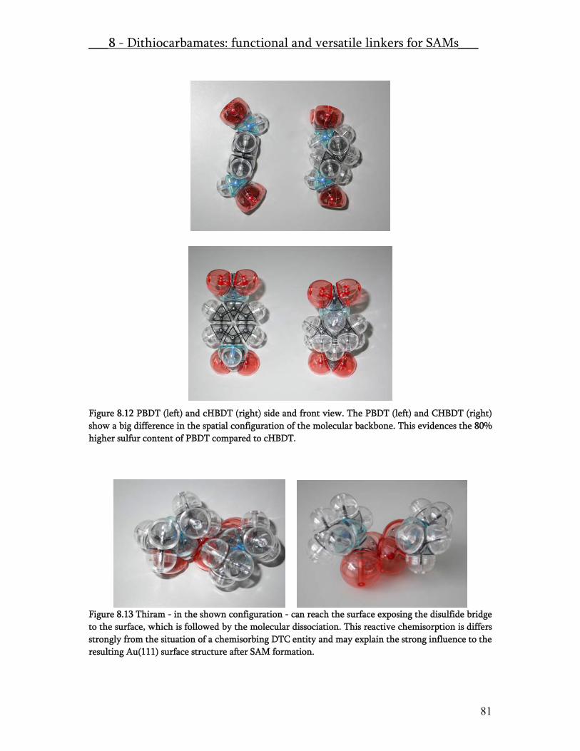
___8 - Dithiocarbamates: functional and versatile linkers for SAMs___
81
Figure 8.12 PBDT (left) and cHBDT (right) side and front view. The PBDT (left) and CHBDT (right) show a big difference in the spatial configuration of the molecular backbone. This evidences the 80% higher sulfur content of PBDT compared to cHBDT.
Figure 8.13 Thiram - in the shown configuration - can reach the surface exposing the disulfide bridge to the surface, which is followed by the molecular dissociation. This reactive chemisorption is differs strongly from the situation of a chemisorbing DTC entity and may explain the strong influence to the resulting Au(111) surface structure after SAM formation.

___8 - Dithiocarbamates: functional and versatile linkers for SAMs___
82
______________________________________________________________________ 1 Frost, D.C.; McDowell, C.A. and Tapping, R.L. J. Electron Spectrosc. Relat. Phenom. 7 (1975) 297.
2 Healy, P.; Myhra, S. and Stewart, A.M. Jpn. J. Appl. Phys. 26 (1987) L1884.
3 Achilleos, A.A.; Gahan, L.R.; Hambley, T.W.; Healy, P.C. and Weedon D.M. Inorg. Chim. Acta. 157 (1989) 209.
4 Ronconi, L.; Maccato, C.; Barreca, D.; Saini, R.; Zancato, M.; and Fregona, D. Polyhedron 24 (2005) 521.

83
9 Supramolecular surface assembly of dithiocarbamates on
Au(111):
Chiral trimeric domains and amorphous structures.
Peter Morf*, Magali Vuaroqueaux†, Florian von Wrochem ‡, Jurina M. Wessels‡ and Thomas A. Jung*.
*Laboratory for Micro and Nanotechnology, Paul Scherrer Institut, 5232 Villigen
Switzerland.
†L2MP-CNRS, Faculté des Science de St. Jerôme, Marseille, France.
‡Sony Deutschland GmbH, Stuttgart Technology Center, Materials Science
Laboratory, Hedelfingerstrasse 61, D-70327 Stuttgart.
Supramolecular chemistry is an area of intense research activities, which has been
inspired by the bottom-up assembly of biologically functional structures.1 The self-
assembly of molecular building blocks is driven by non-covalent intermolecular
forces. The architecture of the building blocks determines shape and functionalities
of the resulting assemblies.1,2 Concepts and principles of supramolecular chemistry
can be applied to three, two and even one dimensional systems as exemplified in
biology for cells, membranes and filaments respectively. Recently two and one
dimensional supramolecular systems have received increasing attention, since
scanning probe techniques offer the exploration of molecular surface arrangements
down to the molecular scale.3
Self-assembled monolayers are two dimensional molecular assemblies at substrate
surfaces which can be formed in ultra high vacuum as well as at the solid liquid

_________9 - Supramolecular assembly of dithiocarbamates_________
84
interface. Molecular adsorption is the initial step of layer formation and can be
followed by a subsequent chemisorption process. Such chemisorbing self-assembled
monolayers (SAMs) often undergo a periodic rearrangement and equilibration of the
molecules consequent to the binding step i.e. the molecular backbone is rearranged
as driven by non-covalent i.e. supramolecular molecule-molecule interactions.
Various chemical functional groups have been introduced so far in order to form
chemisorbing SAMs on metals, semiconductors or on their oxidised surfaces.4 For
many different SAM systems chirality has been observed and has been monitored
for single molecules5 up to full layer assemblies.6
Recently, the formation of SAMs from dithiocarbamates (DTCs) on Au(111) has
been explored in different studies.7 DTCs were found to assemble at the solid liquid
interface in a bidentate state, which is identified by both sulphurs symmetrically
bound to the Au(111) surface. This bidentate bond is potentially the reason for the
novel and very interesting optical and electrical properties of DTCs when
interlinking Au-nanoparticles8 and for the enhanced electronic transport property
found for DTC in mixed thiol/DTC SAMs.9
Herein we present the observation of supramolecular ordering in chemisorbing self-
assembled monolayers formed from sodium diethyldithiocabamate (DEDTC). The
morphology of the DEDTC SAM is compared to the morphology of ammonium
pyrrolidine dithiocarbamate (APDTC) and decanethiol (DT) SAMs on Au(111). The
differences and similarities between the thiol and dithiocarbamate systems on
Au(111) as revealed by X-ray photoelectron spectroscopy (XPS), cyclic voltammetry
(CV), and scanning tunnelling microscopy (STM) are discussed.

_________9 - Supramolecular assembly of dithiocarbamates_________
85
Figure 9.1 shows the anionic part of DEDTC and APDTC. The DTC group, which is present in both molecules defines a plane. If the alkyl chains which are bond to the nitrogen are not positioned within this DTC plane chirality is introduced. Two stable and chiral conformations of DEDTC are illustrated (on the basis of MOPAC calculations) in row a) and b). At room temperature the left handed species of a) can be transformed into the right handed mirror image by a sequential switching process of a methyl group leading to an intermediate form b) and finally by switching the opposite methyl group to obtain the mirror structure. The difference in the heat of formation between form a) and b) is 19 meV and can be thermally inter-exchanged because KBT equals 34 meV at room temperature. Thus DEDTC exhibits a switching chirality and exists as a mixture of a), b), and intermediate forms. The APDTC structure is planar, rigid and achiral.

_________9 - Supramolecular assembly of dithiocarbamates_________
86
In accordance with previous findings DEDTC and APDTC chemisorb on Au(111)
and exhibit only one sulphur surface species, indicating bidentate binding of the
dithiocarbamates7d. DEDTC completely releases the sodium cation during the
assembly process, while in case of APDTC XPS indicates that about 60% of the
ammonium is still present on the surface layer. The quantitative analysis of the
reductive desorption current in CV relative to the sulphur density obtained by XPS
showed that all sulphur atoms are involved in the binding to the gold surface. Thus
the ammonium cation is not expected to be present on the surface but might be
intercalated in the film or adsorbed on the top of the APDTC layer. The relative
surface sulphur density of DT, DEDTC and APDTC is 1 / 1.56 ± 0.19 / 1.95 ± 0.23.
Figure 9.2 a, b and c show high-resolution STM images of APDTC, DEDTC and the
DT reference SAM on Au(111), respectively. While for APDTC (1a) the densely
packed SAM shows no clear ordered superstructure and etch pits, for DEDTC and
DT hexagonally packed SAMs with characteristic etch pit formation can be
observed. DT (1c) shows the well-known ( 3 × 3 )R30°, 2 3 ×3)R30° overlayer
structure, domain boundaries and etch pits.10 The centre to centre lobe distance is
0.50 ± 0.01nm for DT. DEDTC (1b) shows also a hexagonal structure, however, with
a distinctively different lobe size and an average centre to centre distance of 0.98 ±
0.06 nm. The hexagonal packing of DEDTC and DT is also evident in the 2D fourier
transformation spectra of the STM micrograph (Figure 9.2) as well as in the presence
of a 30° rotated hexagonal structure.

_________9 - Supramolecular assembly of dithiocarbamates_________
87
Figure 9.2. Determination of the surface morphology of the dithiocarbamates APDTC (a) and
DEDTC (b) in comparison to DT by scanning tunnelling microscopy (STM). APDTC exhibits a close
to random distribution of molecular size features with some local ordering, while DEDTC and DT
show hexagonal packing. The green hexagons in micrograph b) show different orientation of
domains. Imaging conditions: ambient conditions: APDTC 10 pA, 100mV; DT 2 pA, 100 mV; under
UHV conditions: DEDTC 70 pA, 500 mV. The STM micrographs of the DEDTC SAMs show under
ambient conditions the same structural features (supporting information). The micrographs (a) and
(c) were flattened linearly, while the data of (b) was low-pass filtered.
The comparison of the measured lobe density obtained by STM and the density of S
atoms on the surface the following lobe / molecule relation can be derived: 1 lobe
per 1 DT molecule (per definition), 1 lobe per 3.0 ± 0.5 DEDTC molecules and 1 lobe
per 0.8 ± 0.2 APDTC molecule.

_________9 - Supramolecular assembly of dithiocarbamates_________
88
Figure 9.3 shows zoom images (3.7 x 3.7 nm2), structural molecular models of the sulphur positions and 2D fourier transformation spectra of STM micrographs for DEDTC and (a) and decanethiol (b), respectively. The hexagonal structure is visible for both molecules (green spots) and for DT the
(2 3 ×3)R30° superstructure (red spots) can be found. The fourier transformation spectra for the DEDTC SAM was performed on the data set shown in Figure 9.2 and the rotation of the domains by 30° (blue spots) is clearly visible. Note that the area at full width at half maximum of the lobes in the STM data are 19±8 Å2 for DEDTC and 8±2 Å2 for DT. The area relation is 2.4 : 1.

_________9 - Supramolecular assembly of dithiocarbamates_________
89
In case of DEDTC the measured molecular surface density, the hexagonal packing,
the chirality, and the rather large lobes observed in the STM data, can be explained
by the formation of DEDTC-trimers that are arranged in hexagonal domains. A
similar structure has recently been reported for supramolecular and chiral
assemblies of rubrene.11 We suggest that the formation of these superstructures is
driven by the van der Waals interactions between the ethyl side chains of DEDTC
leading to an asymmetric conformation of the chains. This asymmetric conformation
is stabilised by the interaction of the three molecules and allows for the dense
packing as determined by XPS and CV. The ethyl chains that are attached to the N
atom, conform in two different meta-stable structures, which differ in their heat of
formation by 19 meV (MOPACgas phase, KBT(20°C): 25 meV). As shown in Figure 9.1
top view both forms of DEDTC are chiral after chemisorption on a surface. The close
packing of three molecules into one trimeric complex can introduce, due to the
chirality of the single molecules, two rotational directions on the entire complex as
indicated in the schematic drawing in Figure 9.4. After assembly on a Au(111)
surface the trimeric complex can form domains which exactly represent the
hexagonally closed packed pattern that was observed by STM (Figure 9.4). This way
two chiral complexes can be assembled into two domains, while occupying
equivalent sulphur-gold positions. The 30° rotation of these domains is confirmed in
the experimental data as observed in Figure 9.2b and correspondingly in the 2 D
spectrum of the STM micrograph (Figure 9.3a bottom).

_________9 - Supramolecular assembly of dithiocarbamates_________
90
Figure 9.4 The asymmetric configuration of the ethyl chains of the DEDTC molecules allows the
formation of two trimeric domains with different chirality. The formation of such domains is also
consistent with the experimentally observed hexagonal domains in two phases which are rotated by
30°. The sulphur positions on the Au(111) atomic lattice surface are the same for both chiral
assemblies. This model also conforms to the sulphur density as determined by XPS and CV and
reproduces the measured STM lobe distance. The trimers belong to the C3 point group and the
supramolecular assembly shows a (2 3 × 2 3 )R15° surface structure.
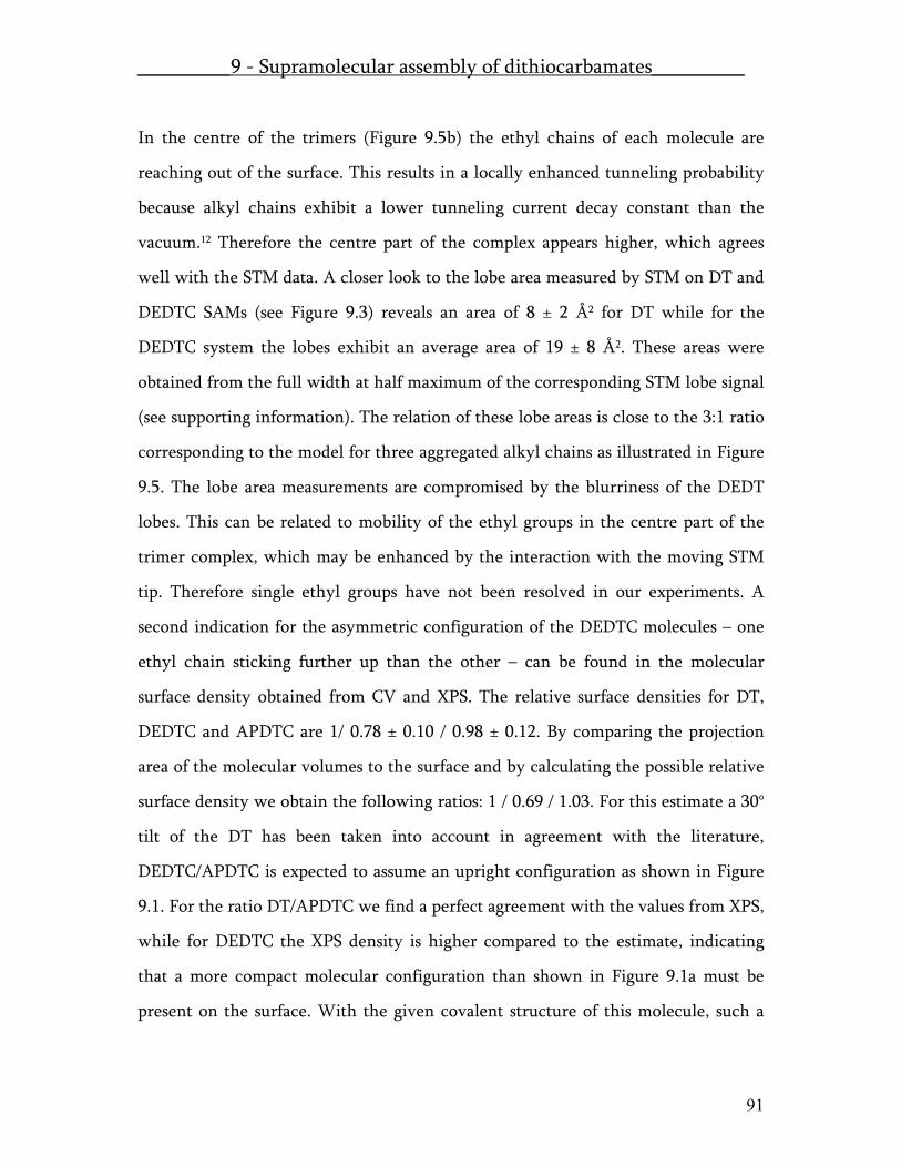
_________9 - Supramolecular assembly of dithiocarbamates_________
91
In the centre of the trimers (Figure 9.5b) the ethyl chains of each molecule are
reaching out of the surface. This results in a locally enhanced tunneling probability
because alkyl chains exhibit a lower tunneling current decay constant than the
vacuum.12 Therefore the centre part of the complex appears higher, which agrees
well with the STM data. A closer look to the lobe area measured by STM on DT and
DEDTC SAMs (see Figure 9.3) reveals an area of 8 ± 2 Å2 for DT while for the
DEDTC system the lobes exhibit an average area of 19 ± 8 Å2. These areas were
obtained from the full width at half maximum of the corresponding STM lobe signal
(see supporting information). The relation of these lobe areas is close to the 3:1 ratio
corresponding to the model for three aggregated alkyl chains as illustrated in Figure
9.5. The lobe area measurements are compromised by the blurriness of the DEDT
lobes. This can be related to mobility of the ethyl groups in the centre part of the
trimer complex, which may be enhanced by the interaction with the moving STM
tip. Therefore single ethyl groups have not been resolved in our experiments. A
second indication for the asymmetric configuration of the DEDTC molecules – one
ethyl chain sticking further up than the other – can be found in the molecular
surface density obtained from CV and XPS. The relative surface densities for DT,
DEDTC and APDTC are 1/ 0.78 ± 0.10 / 0.98 ± 0.12. By comparing the projection
area of the molecular volumes to the surface and by calculating the possible relative
surface density we obtain the following ratios: 1 / 0.69 / 1.03. For this estimate a 30°
tilt of the DT has been taken into account in agreement with the literature,
DEDTC/APDTC is expected to assume an upright configuration as shown in Figure
9.1. For the ratio DT/APDTC we find a perfect agreement with the values from XPS,
while for DEDTC the XPS density is higher compared to the estimate, indicating
that a more compact molecular configuration than shown in Figure 9.1a must be
present on the surface. With the given covalent structure of this molecule, such a
_________9 - Supramolecular assembly of dithiocarbamates_________
92
highly compact configuration precludes conformational adaptation: e.g. by
reorientation of one ethyl chain pointing away from the surface. Taking into
account the rather small interaction energy of the ethyl groups, the supra-molecular
arrangement is expected to be in a very subtle thermal equilibrium. The complex
surface structure of DEDTC on Au(111) consists of chiral domains and inter-domain
regions. Surface water is potentially playing a role, but our conforming observation
of this supramolecular arrangement in the UHV environment (after preparation at
ambient conditions) and in air indicates that the aggregate does not depend on a
high background of water vapour pressure. The reductive desorption characteristic
of DEDTC (supporting information) shows beside the main desorption feature an
additional small peak, which can be attributed to the inter-domain species. Thermal
annealing is introducing disorder and enhances the signal of the inter-domain
species, a behaviour which further supports our assignment of the observed
structure. It is worth to note that the mechanical constraints of the bidentate formed
upon the adsorption of DEDTC on Au(111) is expected to be another determining
factor for the formation of these rather distinct supramolecular aggregates.
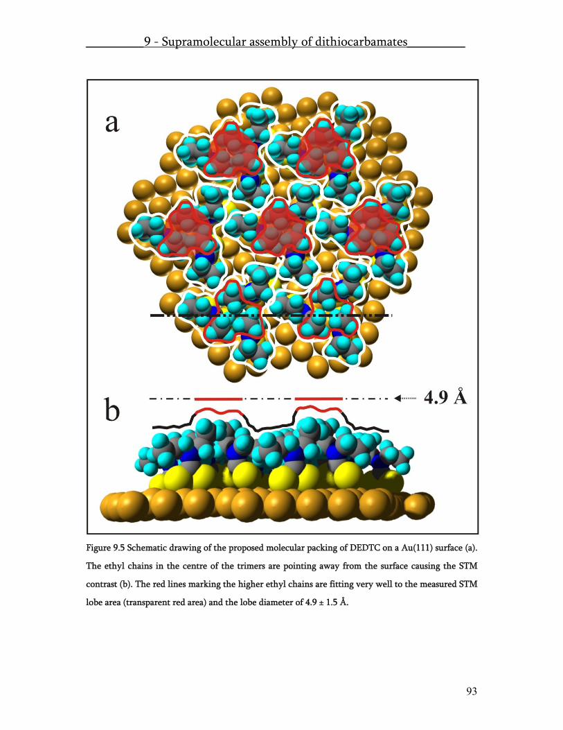
_________9 - Supramolecular assembly of dithiocarbamates_________
93
Figure 9.5 Schematic drawing of the proposed molecular packing of DEDTC on a Au(111) surface (a).
The ethyl chains in the centre of the trimers are pointing away from the surface causing the STM
contrast (b). The red lines marking the higher ethyl chains are fitting very well to the measured STM
lobe area (transparent red area) and the lobe diameter of 4.9 ± 1.5 Å.

_________9 - Supramolecular assembly of dithiocarbamates_________
94
In the case of APDTC we find the STM resolution not sufficient in order to assign
the features of the STM image unambiguously to APDTC or parts of APDTC, e.g. the
Sulphur atoms, nevertheless the average lobe density corresponds reasonably well to
the average APDTC density. The assignment of lobes imaged by STM to
corresponding molecular features and structures closely relates to the question of the
exact imaging mechanism of molecularly resolved STM pictures. Despite of the
manifold of available STM investigations on thiol compounds the STM contrast
mechanism remains under discussion. Different mechanisms for the major
contribution to the tunneling current have been proposed so far: a) tunneling into
the density of states of gold, which is modified by the ad-molecules on the surface,10b
b) tunnelling into the sulphur gold bond13 and c) tunneling directly into the
molecular back bone of the ad-molecules.14 The possibility to differentiate between
different sized thiols in STM data, i.e decanethiol from dodecanethiol15 or from
thiols bearing a ω-hydroxyl group from ω-methyl group,16 indicates that the
tunneling mechanism also includes the molecular backbone.
This agreement of the lobe density and the average number of APDTC molecules
indicates that the electrons tunnel from the tip into the APDTC moiety and not into
the individual S atoms. This is probably due to the fact that both S atoms form a
conjugated electronic structure in combination with the C and N atom of the DTC
binding group.17 The unsharp features in the STM micrograph might relate to the
abundance of the ammonium cation, which has been released from the DTC group
but still is present on the surface (XPS). The intercalation of these ammonium ions
can lower the degree of cristallinity and if not strongly associated to a certain
binding site potentially increases the adsorption of water, which increases the noise
in the STM signal. The STM data were taken under ambient conditions. Long n-
alkanethiols form a perfect hydrophobic layer with a measured contact angle of θd:
_________9 - Supramolecular assembly of dithiocarbamates_________
95
98°± 2° and θs: 94° ± 2°, which usually leads to very nice high resolution images. In
contrast, the SAMs of the here presented DTC compounds have much smaller
contact angles of θd: 57° ± 2°, θs: 56° ± 2° for DEDTC and θd: 40° ± 2°, θs: 40° ± 2° for
APDTC, which raises the possibility to bind adsorbates e.g. a water surface layer.
In conclusion we find that APDTC and DEDTC form densely packed self-assembled
monolayers on Au(111) as revealed by quantititative XPS and CV analysis. For the
DEDTC layer a hexagonal superlattice of trimeric supramolecular aggregates
forming chiral domains is observed, while APDTC shows an irregular pattern of
molecular sized features. The distinctively different ordering of DEDTC and APDTC
is related to the structure of the substituents on the basis of molecular models. The
DEDTC aggregate is to the best of our knowledge the first characteristic
supramolecular assembly observed within a chemisorbing SAM layer. By
comparison of the two systems conclusions about the molecular contrast in STM can
be drawn: APDTC molecules are recognised by a single lobe. This indicates that the
electrons are tunnelling into the molecular backbone. For DEDTC the situation is
more complex. The STM observable lobes are here attributed to a tri-molecular
complex. The DEDTC aggregate therefore provides a basis for the direct comparison
of tunnelling processes taking place in the presence of organic surface layers in
characteristically different arrangements. Next to the interesting electronic
properties of the DTC this is another interesting and novel aspect of DTC binding to
Au(111).

_________9 - Supramolecular assembly of dithiocarbamates_________
96
Experimental Section
SAM preparation
SAM layers of decanethiol (DT) (≥95%), sodium N,N-diethyldithiocarbamate·3H2O
(DEDTC) (>99%) and ammonium pyrrolidine dithiocarbamate (APDTC) (≥98.0%)
(Sigma-Aldrich) were assembled on Au(111) substrates7b using 1mM solutions. DT
and DEDTC where dissolved in ethanol (Fluka, p.a. quality) and APDTC in a 1/1
mixture of H2O (MilliQ) and Ethanol. For all investigations the same substrate
quality and assembly procedures were applied.
XPS-experiments
The XP-spectra were recorded with ESCALAB 220i XL (VG Scientific)
photoelectron spectrometer. The samples were exposed to monochromatic Al K�-
radiation (1486.6 eV) and the spectra were recorded in constant analyser energy
(CAE) mode with analyser path energies of 20 eV for high-resolution spectra. The
sulphur content was determined relative to a full monolayer of DT by normalisation
of the sulphur counts by the counts of the Au4f electrons.18
CV-experiments Electrochemical experiments were performed using a BAS 100a Electrochemical
Analyser with a home built electrochemical cell. As reference electrode a Hg+/HgO
[OH-] system was chosen. Freshly evaporated gold film on mica were punched into
identical round pieces (Ø 8mm) and mounted on a dedicated, gold plated clamp after
preparation. All electrochemical experiments where performed in de-aerated 0.5M
_________9 - Supramolecular assembly of dithiocarbamates_________
97
KOH in aqueous solution. The surface density of molecules was determined from
the desorption charge.7e
STM-experiments
STM experiments were performed using a Nanoscope III Multimode low current
STM and an Omicron UHV-AFM/STM. All measurements were performed with
self-cut Pt/Ir (80/20) tips.
Imaging conditions for the different molecular systems: APDTC 10 pA, 100mV
(Multimode); DEDTC 70 pA, 500 mV (Omicron) and 1 pA 200 mV (Multimode); DT
2 pA, 100 mV (Multimode).
Contact angle measurements
Contact angles were determined for water in the dynamic (θd) and static (θs) mode
on a Krüss surface science system at ambient temperature and humidity conditions.
________________________________________________________________ 1 J-M. Lehn, Supramolecular Chemistry, Concepts and Perspectives, VCH, Weinheim, 1995. 2 J-M. Lehn, Angew. Chem. 1988, 100, 91-116. Angew. Chem. Int. Ed. 1988, 27, 89-112. 3 J.S. Foster, J.E. Frommer, Nature 1988, 333, 542-545. H. Ohtani, R.J. Wilson, S. Chiang, C.M. Mate, Phys. Rev. Lett. 1988, 60, 2398-2401. S. Buchholz, J.P. Rabe, Angew. Chem. 1992, 104, 188-190. Angew. Chem. Int. Ed. Engl. 1992, 31, 189-191. D.P.E Smith, J. Vac. Sci. Technol. B 1991, 9, 1119-1125. J. Frommer, Angew. Chem. 1992, 104, 1325-1357, Angew. Chem. Int. Ed. Engl. 1992, 31, 1298-1328. S. De Feyter and F.C. De Schryver, Chem. Rev. Soc. 2003, 32, 139-150. 4 a) J. Sagiv, J. Am. Chem. Soc. 1980, 112, 92-98. b) R.G. Nuzzo, D.L. Allara, J. Am. Chem Soc. 1983, 105, 4481-4483. c) D.L. Allara, R. G. Nuzzo, Langmuir 1985, 1, 45-52. A. d). Ulman, An Introductionto Ultrathin Organic Films, Academic Press, Boston, 1991. e) A. Ulman, Chem. Rev. 1996, 96, 1533-1554. f) F. Schreiber, Prog. Surf. Sci. 2000, 65, 151-256.
_________9 - Supramolecular assembly of dithiocarbamates_________
98
5 G.P. Lopinski, D.J. Moffatt, D.D.M. Wayner, R.A. Wolkow, Nature 1998, 392, 909-911. 6 S.M. Barlow, R. Raval, Surface Science Reports 2003, 50, 201-341. 7 a) Footnote 30 in C.D. Bain, J. Evall, G.M. Whitesides, J. Am. Chem. Soc. 1989, 111, 7155-7164. b) Th. Arndt, H. Schupp, W. Schrepp, Thin Solid Films 1989, 178, 319-326. c) S. Sánchez-Cortés, C. Domingo, J.V. García-Ramos, J.A. Aznárez, Langmuir 2001, 17, 1157-1162. d) Y. Zhao, W. Pérez-Segarra,Q. Shi, A. Wei, J. Am. Chem. Soc. 2005, 127, 7328-7329. e) P. Morf, F. Raimondi, H-G. Nothofer, B. Schnyder, A. Yasuda, J.M. Wessels, T.A. Jung, Langmuir 2006, 22 658-663. 8 J.M. Wessels, H-G. Nothofer, W.E. Ford, F. von Wrochem, F. Scholz, T. Vossmeyer, A. Schroedter, H. Weller, A. Yasuda, J. Am. Chem. Soc. 2004, 126, 3349-3356. 9 P. Morf et al. submitted. 10 a) C.A. Widrig, C.A. Alves, M.D. Porter, J. Am. Chem. Soc. 1991,113, 2805-2810. b) Y-T. Kim, R.L. McCarley, A.J. Bard, J. Phys. Chem. 1992, 96, 7416-7421. c) G.E. Poirier, M.J. Tarlov, Langmuir 1994, 10, 2853-2856. 11 M-C. Blüm, E. Cavar, M. Pivetta, F. Patthey, W-D. Schneider, Angew. Chem. 2005, 117, 5468-5471. Angew. Chem. Int. Ed. 2005, 44, 5334-5337. 12 L.A. Bumm, J. J. Arnold, T. D. Dunbar, D. L. Allara, P. S. Weiss, J. Phys. Chem. B 1999, 103, 8122-8127. B. Lüssem, L. Müller-Meskamp, S. Kathäuser, R. Waser, M. Homberger, U. Simon, Langmuir 2006, 22, 3201-3027. 13 C. Schönenberger, J. Jorritsma, J.A.M. Sondag-Huethorst, L.G.J. Fokkink, J. Phys. Chem. 1995, 99, 3259-3271. 14 P. Cyganik, M. Buck, W. Azzam, Ch. Wöll, J. Phys. Chem. B 2004, 108, 4989-4996. B. Li, C. Zeng, Q. Li, B. Wang, L. Yuan, H. Wang, J. Yang, J.G. Hou, Q. Zhu, J. Phys. Chem. B 2003, 107, 972-984. 15 L.A. Bumm, J.J. Arnold, L.F. Charles, T.D. Dunbar, D.L. Allara, P.S. Weiss. J. Am. Chem. Soc. 1999, 121, 8017-8021. 16 T. Takami, E. Delamarche, B. Michel, Ch. Gerber, Langmuir 1995, 11, 3876-3881. 17 Thorn, G.D. and Ludwig, R.A. The Dithiocarbamates and Related Compounds, Elsevier, Amsterdam – New York 1962. 18 Briggs, D. and Seah, M.P. Practical Surface Analysis second edition, John Wiley & Sons Ldt., Chichester 1990.

_________9 - Supramolecular assembly of dithiocarbamates_________
99
9.1 Supporting Information
In the XPS data shown in Figure 9.6 only one sulfur species was detected for all the investigated SAMs. The comparison of the XPS sulfur content to the reductive desorption current measured by CV, also shown in Figure 9.6 shows a good agreement. For APDTC we find 1.2 ± 0.2 e / molecule and for DEDTC 0.9 ± 0.2 e / molecule. In the desorption-process one molecule captures one electron. Thus, the molecular surface coverage, determined by XPS and CV agree within the errors.
Figure 9.6 shows XPS and CV signals of DT, DEDTC and APDTC SAMs. The structure related to the measured signals is illustrated in the first row. XPS clearly show one sulfur species for each of this systems and CV reveals reductive desorption waves indicating the chemisorption of the investigated molecules. For DEDTC CV detects a second species at lower desorption potential (circle), which we attribute to a not perfectly ordered inter-domain species of bound DEDTC. Increasing the temperature leads to a stronger pronunciation of the not ordered species what corresponds to the presented model.

_________9 - Supramolecular assembly of dithiocarbamates_________
100
Figure 9.7 shows Nanoscope data of a DEDTC SAM. This measurement was conducted under ambient conditions (1pA, 200mV). The image was more blurry than the data measured in UHV using an Omicron instrument. Nevertheless the hexagonal packing and the inter-lobe distance determined in ambient conditions and in UHV was in perfect agreement.

_________9 - Supramolecular assembly of dithiocarbamates_________
101
Figure 9.8 shows a line scan of a decanethiol SAM. The arrows mark the full width at half maximum. The average value for the STM lob width at half maximum is 0.32 ± 0.05 nm. This leads to an Area of 8 ± 2 Ų.
Figure 9.9 show a 50 nm scan of a DEDTC SAM and three different line scans. The average value of the STM lobe width at half maximum is 0.49 ± 1.5 nm. This leads to an Area of 19 ± 8 Ų. The large error reflects the blurriness of the structure.

102
103
10 Co-assembly – concentration and mixing dependent
binary SAM structures:
Mechanisms of molecular 2D ordering investigated by NEXAFS and STM
Peter Morf*, Frithjof Nolting†, Florian von Wrochem‡, Akos Schreiber‡, Heinz-
Georg Nothofer‡, Akio Yasuda‡, Jurina M. Wessels‡ and Thomas A. Jung*
*Laboratory for Micro and Nanotechnology, Paul Scherrer Institut, 5232 Villigen
Switzerland.
†Swiss Light Source, Paul Scherrer Institut, 5232 Villigen Switzerland.
‡Sony Deutschland GmbH, Stuttgart Technology Center, Materials Science
Laboratories, Hedelfingerstrasse 61, D-70327 Stuttgart.
In this study we have investigated the final molecular structure of mixed self-
assembled monolayers (SAMs) formed at the solid liquid interface and the structural
dependence on the initial mixing ratio and net concentration of two mixed thiol
_10 - Co-assembly – concentration and mixing dependent binary SAMs_
104
species. Clean Au(111) surfaces were exposed to mixtures comprising a non polar
(decanethiol) and a strong polar (1,4-bis(mercaptoacetamido)benzene) compound.
On parallel processed SAM samples the average composition and orientation was
investigated by near edge X-ray absorption fine structure (NEXAFS) spectroscopy
and complementary data such as the surface morphology were obtained by scanning
tunnelling microscopy (STM). The resulting surface structure strongly depends on
the total concentration of the initial mixed solution and the initial mixing ratio of
the molecules. We found completely disordered structures as well as fully ordered
and oriented layers composed of domains of dense packed decanethiol surrounding
molecular Islands of the aromatic and polar dithiol compound. In order to ensure
the formation of stable and well defined island structures the mixing ratio of the
polar vs. the nonpolar thiol species should be lower than 1/9 not exceeding a net
concentration of 0.1 mM. Finally A very interesting effect was found for low
contents of the polar compound. The polar compound did not appear on the
resulting surface i.e. was completely removed from the surface, but the residual
alkanethiol SAM exhibited larger etch-pit and domain structures than a SAM
formed from a pure solution. Thus we assume the polar compound to interact
strongly with the alkanethiols and the Au(111) surface in the fast initial assembly
step and the subsequent thermal equilibration. In our model we show how the polar
compound if applied in very low concentrations is preventing parts of the

_10 - Co-assembly – concentration and mixing dependent binary SAMs_
105
alkanethiol molecules of being kinetically trapped into small domains and how the
same compound if applied in higher concentrations is partially inhibiting the
ordering of the DT layer.
1. Introduction
Nanotechnology and related surface structuring techniques can be divided mainly
into two different approaches: the top-down and the bottom-up strategy. The
promising ease of surface modification using self-assembled monolayers (SAMs) in
nanotechnology,1,2 which is a possible bottom-up system, has not yet been
transferred into technological patterning. The top-down technologies as Micro
contact printing (μcP),3,4 nanografting5,6 and dip-pen nanolithography7,8 by AFM are
also using self assembled monolayers but not their self- structuring abilities, just the
paint like layering and binding behaviour of thiols on metals was used. This study is
motivated by the need for deeper understanding of monolayer self-structuring to
exploit self-assembly as bottom-up self-patterning systems. Self-patterning has been
demonstrated in UHV9 but has not yet been established by assembly from
solution.10 Self-assembly out of solution showed phase separation for alkanethiols
mixed with ω-substituted alkanethiols11 as well as for amide-groups containing
thiols.12,13

_10 - Co-assembly – concentration and mixing dependent binary SAMs_
106
In our investigation we focused on binary assemblies on Au(111) formed from
solutions containing 1,4-bis(mercaptoacetamido)benzene (DMAAB) and decanethiol
(DT). It is the aim of this study to show (I) the different structural ordering
phenomena depending on molecular mixing and net concentration of the assembly
solutions and (II) the powerful combination of near edge X-ray absorption fine
structure (NEXAFS) spectroscopy and scanning tunnelling microscopy (STM). The
molecular composition and orientation can be detected by NEXAFS,14 whereas STM
can resolve nanometer sized structures on thiolate monolayers15 and draw a
morphological local picture of the assembly. NEXAFS is an averaging technique
measuring on a macroscopic spot (0.5x0.5 mm2). The information on the orientation
and composition of the molecules are averaged over a huge amount of about 1014
molecules. STM in comparison reveals very local information (~0.1 Å) but does not
contain direct information on the spatial orientation and conformation of the ad-
molecules. Only if the molecules are flat lying on the surface STM is able to directly
detect it.16 The well-know tilt of alkanethiol SAMs on metal cannot be acquired by
STM, even if SAM superstructures can be imaged.17 Thus the combination of
NEXAFS and STM is ideal to investigate the self-assembly processes and resulting
structures on monolayer systems.
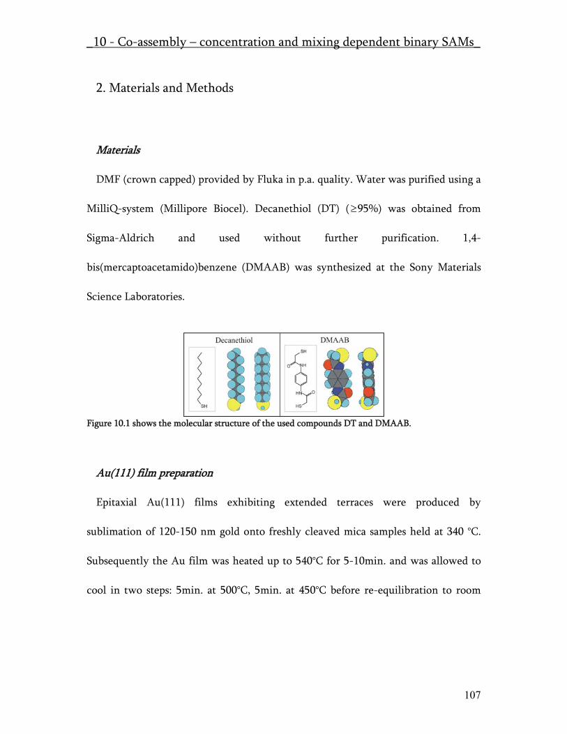
_10 - Co-assembly – concentration and mixing dependent binary SAMs_
107
2. Materials and Methods
Materials
DMF (crown capped) provided by Fluka in p.a. quality. Water was purified using a
MilliQ-system (Millipore Biocel). Decanethiol (DT) (≥95%) was obtained from
Sigma-Aldrich and used without further purification. 1,4-
bis(mercaptoacetamido)benzene (DMAAB) was synthesized at the Sony Materials
Science Laboratories.
Figure 10.1 shows the molecular structure of the used compounds DT and DMAAB.
Au(111) film preparation
Epitaxial Au(111) films exhibiting extended terraces were produced by
sublimation of 120-150 nm gold onto freshly cleaved mica samples held at 340 °C.
Subsequently the Au film was heated up to 540°C for 5-10min. and was allowed to
cool in two steps: 5min. at 500°C, 5min. at 450°C before re-equilibration to room

_10 - Co-assembly – concentration and mixing dependent binary SAMs_
108
temperature. This annealing procedure reproducibly lead to uniform surfaces
exhibiting characteristic triangular (111) terraces typically 200 x 200 nm2 in size.
SAM preparation
DT SAM layers were assembled by exposure of the freshly evaporated gold
substrate to thiol solutions of the pure and the mixed systems. The solutions
exhibited 1mM or 0.1 mM concentration. Both molecular compounds were solvable
in DMF and therefore the assembly process was conducted in DMF for 24h. The
glass ware was cleaned before use in piranha solution (1/3, H2O2 30%/H2SO4 96%) –
to handle with care!
Table 10.1 shows the composition of the solutions used in this study to fabricate mixed SAMs.
Sample a b c d e
DT [mM] 1 0.9 0.09 0.099 0.0999
DMAAB [mM] 0 0.1 0.01 0.001 0.0001
DMAAB/DT 0 1/9 1/9 1/99 1/999

_10 - Co-assembly – concentration and mixing dependent binary SAMs_
109
STM-experiments
STM measurements were carried out using a Nanoscope III Multimode low
current STM. Tunnelling current and bias potential where kept at 2 pA and 100 mV.
Pt/Ir wire (0.25 mm diam.) was used to cut non-oxidising sharp tips.
NEXAFS-experiments
NEXAFS experiments were performed at the Surface/Interface Microscopy (SIM)
beamline of the Swiss Light Source, Paul Scherrer Institute. The spectral resolution
at 300 eV photon energy is around 60 meV (resolving power 1/5000) and the linear
polarization degree is 98%. The orientation of the linearly polarized X-rays can be
varied between 0 and 90 degree enabling the measurement of orientation effects
without the need to rotate the sample. The NEXAFS spectra were taken with the
total electron yield (TEY) detection, which is ideally suited for the measurement of
thin films due to the small electron escape depth of typically less than a few
nanometers. The samples were mounted in a vacuum chamber, which was not at the
focus point of the beamline resulting in spot size of approximately (0.5 * 0.5) mm.
The TEY signal was obtained by measuring the sample photocurrent with a
picoamperemeter. The final resulting signal was obtained by normalizing the sample
TEY signal to the equally measured TEY signal of a freshly prepared reference gold
sample. In this way information about the composition of the film is obtained, since
_10 - Co-assembly – concentration and mixing dependent binary SAMs_
110
for example the benzene π* excitation occurs at energies of 285.0 eV18 and
resonances related to the alkyl chains occur at 287.5 eV19 for mixed Rydberg states
and at 293.0 eV for the σ* (C-C) excitation.20 In order to determine the orientation of
the monolayers compounds one has to employ X-ray linear dichroism. Therefore,
the sample surface normal was tilted by an angle of 70° to the incident beam. Using
vertically linearly polarized light one probes the in-plane orientation whereas
horizontally linearly polarized light probes the out-of-plane components. The
dichroism is then calculated XLD° = (Teyin-plane° – Teyout-of-plane°)/(Teyin-plane° + Teyout-of-
plane°). The size of the dichrosim can be interpreted as a measure of the average
ordering of molecular bonds i.e. unoccupied molecular orbitals. Such an
interpretation allows for the determination of the orientation of molecular
structures within a monolayer.
3. Results and Discussion
3.1 Detection of the Molecular composition and orientation
NEXAFS spectroscopy was performed on the SAM samples in order to obtain the
average molecular ordering i.e. the average molecular tilt as well as the molecular
compositions. NEXAFS at the carbon K-edge at photon energies around 280 eV tests
electron transitions from the carbon 1s state into unoccupied molecular states by X-
rays. The 1s state is spherical symmetric and usually excited molecular orbital states

_10 - Co-assembly – concentration and mixing dependent binary SAMs_
111
are not. Therefore the transition probability C1s → Mo* is depending on the
polarization of the incoming photon i.e. the direction of the electric field vector.
Thus the polarization dependence of the X-ray absorption characteristics allows the
detection of the average molecular orientation. On the top of Figure 10.2 we show
NEXAFS results of two selected samples. On the left a pure and well-studied DT
SAM (a) is compared to a mixed SAM (c) on the right side (solution: DT/DMAAB :
9/1, net conc. : 0.1 mM). In the 90° (in-plane) absorption spectra one clearly detects
the strong resonance of mixed Ryberg states related to the alkyl chain at 287.5 eV
(green line). At higher energies the much broader alkyl chain σ* (C-C) excitation at
293.0 eV occurs.21 Whereas sample (a) only shows the two alkyl chain signals we
were able to detect an additional peak for sample (c). This signal at 285 eV (red
circle) can be attributed to the π* resonance of benzene. This proofs the abundance
of a DMAAB surface species after the assembly process. The dichroism signal –
reflecting the normalised signal difference measured at differing polarization – for
the two systems is plotted in Figure 10.2 just below the absorption spectra. The
stronger the dichroism signal for the excitation of the mixed Rydberg states is the
more perpendicular is the average orientation of the alkyl chains to the surface. The
DT SAM shows a strong dichroism signal, which indicates a densely packed alkyl
chain structure tilted by an angle of 32-35°.22,23 The average tilt angle with respect to
the surface normal of the DT-alkyl chains in mixed systems as in the SAM on sample

_10 - Co-assembly – concentration and mixing dependent binary SAMs_
112
(c) is higher than for the pure DT-SAM, which indicates that DMAAB inhibits the
close packing of DT molecules.
3.2 Characterizing the 2D-morphology
Since the local ordering of the monolayers can not be obtained by NEXAFS
spectroscopy, we performed STM on parallel processed samples as used for the
NEXAFS investigations. In Figure 10.2 two 50 x 50 nm2 STM micrographs are
presented in the centre part of the graph. The DT SAM exhibits the standard thiol
features: crystalline domains24 (white line), domain boundaries25 – separating the
domains – and vacancy islands26,27 (dark spots, “etch-pits”). The STM micrograph of
SAM sample (c) differs significantly. Only a few crystalline domains (white lines)
and smaller etchpis are present. Unordered regions exhibiting a higher degree of
roughness are mainly covering the surface and new structural features – molecular
islands (white circle) – can be found. It is an interesting finding that DMAAB islands
are never observed within the crystalline DT domains. The DMAAB islands appear
brighter (higher) in the STM micrograph, which is due to the higher electron
tunneling probability through aromatic structures compared to alkyl chains. The
unordered regions on the gold surface may now partially contain well packed DT
and DMAAB as well as flat lying molecules. Such a molecular arrangement results in
a high STM roughness.
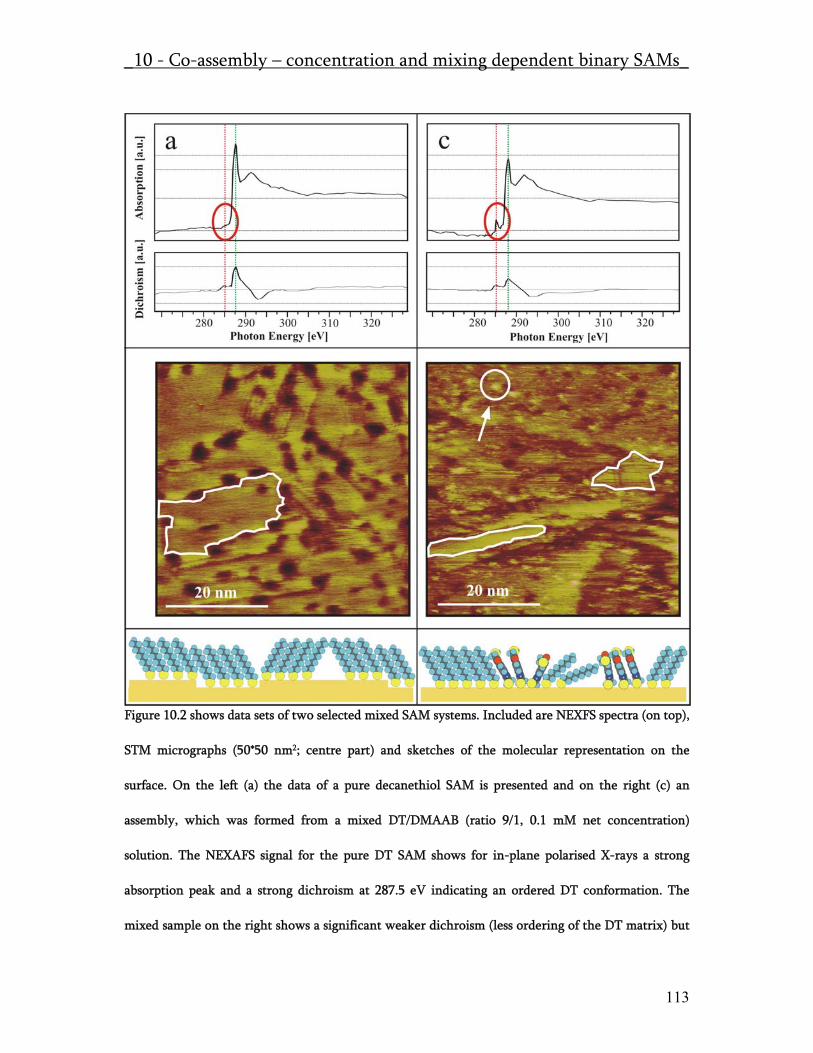
_10 - Co-assembly – concentration and mixing dependent binary SAMs_
113
Figure 10.2 shows data sets of two selected mixed SAM systems. Included are NEXFS spectra (on top),
STM micrographs (50*50 nm2; centre part) and sketches of the molecular representation on the
surface. On the left (a) the data of a pure decanethiol SAM is presented and on the right (c) an
assembly, which was formed from a mixed DT/DMAAB (ratio 9/1, 0.1 mM net concentration)
solution. The NEXAFS signal for the pure DT SAM shows for in-plane polarised X-rays a strong
absorption peak and a strong dichroism at 287.5 eV indicating an ordered DT conformation. The
mixed sample on the right shows a significant weaker dichroism (less ordering of the DT matrix) but

_10 - Co-assembly – concentration and mixing dependent binary SAMs_
114
an additional aromatic peak at 285 eV evidencing the presence of DMAAB. The STM micrographs
show typical features for the pure DT SAM. Crystalline domains (white line), domain boundaries
(dark lines between the domains) and etch-pits (dark vacancy islands) are present on the surface. The
mixed system looks very different. Only partial formation of crystalline domains (white line) was
visualized by STM. Mixed and rough structures dominated the surface while small islands (white
circle) appeared as a new structural feature.
3.3 Mixed SAMs
In Figure 10.3 we present all the relevant NEXAFS and STM data to present the
significant dependence of the final SAM structure on the mixing ratio of DMAAB to
DT and on the net concentration of the initial SAM forming solution (Table 10.1).
In the NEXAFS data we detected for sample (b)-(d) aromatic absorption signatures
(red circle), which are not present on sample (a) the pure DT-SAM and on sample
(e), where the SAM was formed from a solution with high DT and very low
DMAAB content. The relative aromatic signal intensity varies in the following
relations as denoted in Table 10.2.: Iarom(d) < Iarom(b) < Iarom(c). This result seems to
contradict the relative DMAAB content in the initial SAM forming solution. But if
we take into account that the upright molecule contributes more to the absorption
signal at 285 eV we understand, that sample (c) has the higher degree of oriented
DMAAB molecules compared to the sample (b). The NEXAFS dichroism signal at

_10 - Co-assembly – concentration and mixing dependent binary SAMs_
115
288 eV (dotted line) over all samples is monotonically increasing at either lower
DMAAB concentration or lower net concentration of the initial solution. This
increasing signal is directly connected to the more upright conformation of the DT
molecules i.e. their alkyl backbone. The STM micrographs reveal exactly the same
tendency. Islands are present on the surface whensoever in the NEXAFS spectra the
aromatic feature was detected. Regarding the sample sequence (b), (c), (d) the island
size and number changes from bigger to smaller and from “many” to “few” as
denoted in Table 10.2. The lower the DMAAB content and the lower the net
concentration the more crystalline DT-SAM structure were formed. An appropriate
representation of the degree of the SAM surface crystallinity is the line scan
roughness. Representative line scans are shown in Figure 10.3 below the STM
micrographs. The abundance of etch-pit structures on all samples can be seen in the
line scans as line depressions of 2.4 Å. The etch-pit features in the line scans of
Figure 10.3 are show in blue color and have to be separated from the regular SAM
roughness. The changing SAM roughness is represented on the bar below the line
scan, where the smooth regions (black bar) and the rough regions (grey) are
separately specified. The increasing black bar is representing the increasing
abundance of crystalline DT-SAM domains starting from sample (b) exhibiting no
crystalline domains and no smooth (black) regions and ending with sample (e) were
a complete smooth SAM surface was formed.

_10 - Co-assembly – concentration and mixing dependent binary SAMs_
116
If the surface concentration of DMAAB is exceeding a critical value the molecular
ordering of the whole SAM is completely inhibited. This can be attributed to the
strong and directional molecular dipoles of the amide group present in the DMAAB
molecule which can introduce a relative intermolecular tilt not allowing the
formation of a proper pi-pi stacking of the benzene systems. Also the possibility to
bind with both thiol groups to the gold surface28 may introduce disorder and can
prevent DMAAB and DT molecules to line up. Comparable investigations on pure
DMAAB layers exhibited weak NEXAFS dichroism and a very rough STM surface as
presented in the supplementary information. Such a weak NEXAFS dichroism can
be interpreted as a sign for an average molecular orientation at an angle closely to
54.7°. For this “magic angle” NEXAFS dichroism vanishes for any system.14 A similar
SAM system as DMAAB on gold exhibited also a very low dichroism signal, which
was taken as a sign for the molecular tilt to be close to the “magic angle”.29 Another
possible interpretation for a vanishing NEXAFS dichroism is the complete random
orientation of the DMAAB molecules (vide supra). The random orientation of
DMAAB would also be supported by the rough surface structure found by STM.

_10 - Co-assembly – concentration and mixing dependent binary SAMs_
117
Figure 10.3 NEXAFS and STM on different mixed SAMs. In the top row the absorption spectra for in-plane polarised X-rays and dichroism signals are shown. The absorption spectra clearly reveal the presence of DMAAB on SAM (b), (c), and (d) (aromatic signal at 285 eV, red circle). On the samples (a) and (e) no aromatic peaks are visible in the NEXAFS spectra. The dichroism signal indicates a clear disorder/order dependence on the concentration and mixing ratio of the initial thiol solutions: the lower the DMAAB concentration, the more the DT structures are ordered. And additionally a higher degree of ordering occurs at lower concentrations (1 mM (high conc.) vs. 0.1 mM (low conc.)). The 150 nm x 150 nm STM micrographs also exemplifies significant morphological differences between the samples (a) to (c). On the pure DT SAM (a) we find smooth regions and etch-pits (dark spots). On sample (b) almost no regular structures (no clearly defined etch-pits, no smooth regions) can be found. Many bright islands (white circle) are present on this very rough surface. The roughness is illustrated in the line scan below the STM micrograph. Sample (c) shows an interesting intermediate state of ordering: smooth regions (black area) are alternating with rough regions. This can be seen in the line scan across crystalline regions (black) and low ordered regions (gray). Many small islands (white circle) are formed on the surface of sample (c). On sample (d) only a few islands are found (white circle) and beside the etch-pits only smooth regions are visible. The sample (e) is similarly structured to a pure DT SAM. The significant larger and structurally differing etch-pit structures on SAM (d) and (e) compared to SAM (a) may be explained by the small but determining

_10 - Co-assembly – concentration and mixing dependent binary SAMs_
118
abundance of DMAAB interfering with the DT molecules in the initial SAM-forming state. At the bottom a molecular model shows the structural features found for the different samples.
Sample (c) shows an intermediate state of organisation between a complete
ordered and disordered surface layer. A smother over-all surface compared to
sample (b) (line scan) could be detected including some crystalline decanethiol
domains (white areas) and many small islands (white circle). The line profile shows
different crystalline smooth regions (black bars) and mixed not ordered rough
regions (grey bars).

_10 - Co-assembly – concentration and mixing dependent binary SAMs_
119
Table 10.2 Structural features found in STM and NEXAFS of mixed DMAAB/DT SAMs.
Sample a b c d e
STM
DT-SAM
crystallinity
100 % 0 % 10 % ~ 100% 100%
DMAAB
island size diam.
- 3 ± 0.5 nm 1.5 ± 0.5 nm 1.5 ± 0.5 nm -
DMAAB
Islands [#/μm2]
0 12’000 33’000 450 0
DMAAB
Island area
0 9 ± 3 % 6 ± 2 % 0.08 ± 0.03 %
Net etch-pit area 15 ± 3 % 12 ± 3 % 11 ± 3 % 11 ± 3 % 12 ± 3 %
Etch-pit diam. 3.7 ± 2.3 nm 2.8 ± 1.9 nm 2.0 ± 1.5 nm 4.2 ± 3.4 nm 4.5 ± 3.0 nm
NEXAFS
rel. aromatic content (peak hight at 285 eV)
0 1.0 (def.) 1.3 0.7 0
rel. DT-SAM orient-tation dichroism at 287.5 eV
1.0 (def.) 0.3 0.5 0.9 1.0

_10 - Co-assembly – concentration and mixing dependent binary SAMs_
120
3.4 Mechanism of Mixed SAM-formation
Figure 10.4 shows the most dominant processes and effects, which are determining the layer growth and its final structure. The first step of the SAM formation includes the diffusive transport of thiols to the surface (b), the physisorption (c1) and the subsequent chemisorption (c2) onto the Au(111) surface. Thereby the solvation shell (a, solvent: DMF) must be partially released. The chemisorbed molecules may desorbe (d) and readsorb, laterally diffuse on the surface with (e2) or without (e1) neighbouring gold atoms. And even gold atoms itselves may show diffusive mobility. The molecular interaction by electrostatic or van der Waals forces (f) comes into play at higher surface coverage and finally leads to the formation of dense pure, mixed or phase separated assemblies.
The quantification of the resulting surface structures of the mixed assemblies as
shown in Table 10.2, allows for a deeper analysis and understanding of the basic
processes in the mixed SAM formation. First we like to summarise reports from the
literature on the different steps in the formation of pure and mixed thiol SAMs on
Au(111) to allow for a better discussion of our findings and results. In Figure 10.4
_10 - Co-assembly – concentration and mixing dependent binary SAMs_
121
the most important processes involved in the SAM formation from thiol solution are
illustrated.
The formation of mixed SAMs can be divided into five major process steps:
i) The first process step includes the diffusive motion of the solved molecules and
the related solvation shell (a) toward the Au(111) surface. The adsorption process for
alkanethiols assembled from solutions exhibiting concentrations of 1-0.01 mM can
successfully be described by the Langmuir adsorption isotherm, thus diffusion
limitation does not play a role.30,31 For lower thiol concentrations such as equal or
below 1μM the process of layer formation appears to be diffusion limited.32,33,34
Others reported that for decanthiol concentrations of 0.1 μM only the “down
laying”, striped phase was observed as for the slightly enhanced concentration of 0.3
μM island formation was taking place.35,36 In their experiments the phase formation
was reported on a timescale of minutes to hours, which is much longer than for a
1mM assembly process.
ii) Molecules are stochastically approaching the surface.31,33 Since a molecule collides
with the surface it is either reflected on the surface or initially undergoes a
physisorption process and occasionally in a second step it chemisorbs.37
A measure for the adsorptive strength of a molecule to a specific surface is
expressed by the sticking coefficient. The sticking coefficient displays the ratio of
_10 - Co-assembly – concentration and mixing dependent binary SAMs_
122
the number of events were potential adsobate collides with the surface and the
number of events were adsorption is taking place. The sticking coefficient equals
unity for adsorption of alkanethiols out of the gas phase but is much smaller for the
assembly from liquids.33 Because of the influence of the solvent shell onto the
adsorption energetics. For the adsorption process from solution the equilibrium of
entropic and enthalpic contributions is very subtle. Thus the free energy of
adsorption of 1-ocdadecanthiol from n-hexane solution is only in the range of
hydrogen bonding in liquid alcohols.31
iii) The third step comprises the establishment of an absorption/desorption
equilibrium.38-42 Such equilibria exists for all SAM structures in solution at activated
sites as vacancy island or crystalline domain borders. Thus the choice of a specially
fitting solvent under which well prepared SAM samples can be stored can pushes
the equilibrium to the side of the adsorbed form and prevent desorption and
oxidation at the same time.43
iv) The chemisorbed molecules perform lateral motion (e1) on the surface or in the
case of the dithiol DMAAB the subsequent chemisorption process with the second
thiol group may lead to a flat lying double bonded species. The formation of the flat
lying structure also observed for alkanethiols occurs in this step.44 The molecular
diffusion might also be accompanied by the motion of gold atoms (e2, e3), which
leads to the formation of vacancy islands (“etchpits”).31,45 The growth of the vacancy

_10 - Co-assembly – concentration and mixing dependent binary SAMs_
123
islands in vacuum and from solution usually is initiated as the Au(111)
reconstruction vanishes and undergoes an ostwald ripening process, where small
vacancies coalesce into larger ones.44 These vacancy islands can thermally be healed
out.46 Poirier et al. achieved the formation of extremely large decanethiol domains
on a Au(111) single crystal surface exhibiting no vacancy islands at all by thiol
dosing via the gas phase at normal pressure at slightly elevated temperatures.47 This
achievement illustrates the subtle balance between the kinetically trapped – vacancy
islands containing surface – and the well equilibrated vacancy free surface.
v) The last step of pure and mixed layer formation consists of the lateral molecular
motion, which leads to collisions of the chemisorbed molecules.The more molecules
adsorb on the surface the more upright and crystalline domains evolve. Coulomb or
van der Waals forces start to monitor the molecular interactions (f), which lead at
about 0.8 coverage to slower growth rates33 but finally stable and energetically
favorable assemblies. Whereas the first four assembly steps for solution
concentrations of 0.1 mM solutions take a few minutes to take place. The last step,
which is the final re-organization of the molecular backbones, needs hours to days.
The basic cause whether two molecular species – initially mixed in the assembly
solution – exists as intermixed, separated or excluded phases on the surface depends
mostly on the interaction between the molecules.40,41,48,49

_10 - Co-assembly – concentration and mixing dependent binary SAMs_
124
The samples prepared for this study were assembled for 24h and we assume that if
no equilibrium then a quasi static assembly structure was reached.
The most important results characterizing the samples (a) to (e) are collected in
Table 10.2. One of the most interesting features of the presented data is the almost
constant total area of vacancy islands over the whole series. Thus we can conclude
that the gold diffusing around whilst forming the vacancies do not much depend on
the thiol species. On the other hand we see that the average size of the vacancies
depend strongly on the composition i.e. relative and absolute concentration of the
two mixed species. The most interesting result emerges when sample (a) and sample
(e) are compared. Here we do not see a difference on the resulting molecular
composition of the layer – both layers consist of pure decanethiolate. But the size of
the vacancy island and the size of the crystalline domains differ significantly.
Additionally the crystalline domains, as shown in the supporting information,
exhibit the c(4×2) superstructures without thermal annealing, which is a sign for
better equilibration of the layer. We attribute this phenomenon to the small portion
of DMAAB molecules initially assembled out of the solution and finally being
removed from the surface, because even if low concentrated in the initial solution
the probability to reach the surface is high enough. The presence of DMAAB
hinders the DT to form smaller domains because the number of initial and stable
growth DT sites is limited. Therefore the DMAAB has a strong impact on the
_10 - Co-assembly – concentration and mixing dependent binary SAMs_
125
assembly of the decanethiol and the possible ostwald ripening of the vacancy island
as sketched in Figure 10.5. Most probably it occurs an ostwald ripening process
because we detect almost the same net area of vacancies on all samples and only the
average size significantly increased from sample (a) with 11 nm2 pit area to sample
(e) with 16 nm2 pit area. In addition the error reflecting the size distribution of the
vacancies increased for sample (e) compared to sample (a), which evidences the
evolution from smaller to bigger islands. In the supporting information additional
STM micrographs are shown to further exemplify this argument.
If we now move our focus to the features expressed by the presence of DMAAB
molecules, recognized by the bright features in STM, we remark that for the sample
(b) the surface area, which is covered by DMAAB islands, is slightly larger than for
sample (c). Additionally the average island size is 3 ± 0.5 nm and 1.5 ± 0.5 nm,
respectively. Taking into account that the intermolecular spacing of DMAAB equals

_10 - Co-assembly – concentration and mixing dependent binary SAMs_
126
Figure 10.5 shows the mechanisms, which lead to large decanethiol domains and to ostwald ripening of the vacancy islands (“etch-pits”). The low density of DMAAB molecules do not form stable islands structures. As the DMAAB molecule is strongly polar compared to DT the DMAAB molecules are not included into the molecular arrangement of DT but serves as a seed were the DT domains grow (a). The normal DT domain growing process (b) occurred also on the sample (e) but the process (a), (c) and (d) lead to ostwald ripening of the vacancy island as to the increased domain size. Finally the DMAAB are expulsed from the surface (e).
the usual assembly distance of benzenethiol,50 which is 0.5 nm, we find as an
average number of molecules composing the island for sample (b) 32 and for sample
(c) 8 molecules. The most interesting finding in this context is that for sample (d)
only a few islands were found but the average island size was 1.5 ± 0.5 nm as for
sample (c). On sample (e) no island was found suggesting that for the formation of
DMAAB islands only a minimal island size remains stable during the whole
assembly process. Thus the DMAAB molecules once clustered to groups of 8
molecules cannot be removed from the surface by decanethiol anymore. This
finding is also suggested by the fact that DMAAB islands are exclusively placed at

_10 - Co-assembly – concentration and mixing dependent binary SAMs_
127
the border of DT domains, which is due to the non-mixing molecular properties, but
illustrated that the growth of decanethiol domains do not surround DMAAB island.
Thus the DT domain growth has to stop or the DMAAB island to be removed.
4. Conclusion
We have shown that the final structure of mixed self-assembled monolayers on
Au(111) strongly depend on the initial mixing ratio and net concentration of the
assembly solution. The combination of NEXAFS and STM has exemplified to be a
very powerful tool for the investigation of mixed SAM structure formation. The
complementary information on the average surface composition and orientation
accessed by NEXAFS and the local ordering detected by STM allows for thorough
analysis monolayer systems.
For the mixed assembly of a strongly polar (DMAAB) and a nonpolar (DT)
compound from solution onto a Au(111) surface we found a critical concentration
for the polar DMAAB compound. When this critical concentration was exceeded
no proper molecular ordering also of the decanethiol majority was possible anymore.
Well defined DMAAB islands surrounded by an ordered DT-SAM is spontaneously
formed out of a solution exhibiting higher mixing rations than 10/1 for DT/DMAAB
and lower net concentration than 10-4 M. DMAAB islands are exclusively placed at
the border of DT domains. If the DMAAB concentration was lower than 0.1 % in
_10 - Co-assembly – concentration and mixing dependent binary SAMs_
128
the initial solution no DMAAB structures were detected on the surface anymore,
neither by NEXAFS nor by STM. Nevertheless the resulting DT SAM differed
significantly from a DT SAM formed from a pure DT solution. The vacancy islands
were undergoing ostwald ripening i.e. the net vacancy area remained constant but
the individual island exhibited a larger area. Additionally the DT domains were
growing much larger compared to the pure layer and exhibited the c(4×2)
superstructures without thermal annealing, which is a sign for better equilibration
of the layer. This can be explained by the fact that low concentration of DMAAB on
the surface supports the crystallization process of DT as it is not good solvable
within the alkyl chains but acts as an adsorbate intermediate as shown in our model,
which finally is completely removed from the surface.
Acknowledgement
This work was financially supported by Sony Deutschland GmbH – Materials
Science Laboratory. T.J. acknowledges financial contributions from the Swiss
National Science Foundation and the NCCR Nanosciences. Part of this work was
performed at the SLS, Paul Scherrer Institut, Villigen, Switzerland.
______________________________________________________________________ [1] Love, J.C.; Estroff, L.A.; Kriebel, J.K.; Nuzzo, R.G.; Whitesides, G.M. Chem. Rev. 2005, 105, 1103.

_10 - Co-assembly – concentration and mixing dependent binary SAMs_
129
[2] Chen, D.; Li, J. Surf. Sci. Rep. 2006, doi:10.1016/j.surfrep.2006.08.001
[3] Xia, Y.; Mrksich, M.; Kim, E.; Whitesides, G.M. J. Am. Chem. Soc. 1995, 117, 9576.
[4] Kumar, A.; Whitesides, G.M. Appl. Phys. Lett. 1993, 63, 2002.
[5] Xu, S.; Liu, G-Y. Langmuir 1997, 13, 127.
[6] Amro, N.A.; Xu, S.; Liu, G-Y. Langmuir 2000, 16, 3006.
[7] Piner, R.D.; Zhu, J.; Xu, F.; Hong, S.; Mirkin, C.A. Science 1999, 283, 661.
[8] Ginger, D.S.; Zhang, H.; Mirkin, C.A. Angew. Chem. Int. Ed. 2003, 43, 30.
[9] de Wild , M.; Berner, S.; Suzuki, H.; Yanagi, H.; Schlettwein, D.; Ivan, S.; Baratoff, A.; Guentherodt, H-J.; Jung, T.A. Chem. Phys. Chem. 2002, 3, 881.
[10] Smith, R.K.; Penelope, A.L; Weiss, P.S. Prog. Surf. Sci. 2004, 75, 1.
[11] Stranick, S.J.; Parikh, A.N.; Tao, Y-T., Allara, D.L.; Weiss, P.S. J. Phys. Chem. 1994 98, 7636.
[12] Smith, R.K.; Reed, S.M.; Lewis, P.A.; Monnell, J.D.; Clegg, R.S.; Kelly, K.F.; Bumm, L.A.; Hutchinson, J.E.; Weiss, P.S. J. Phys. Chem. B 2001, 105, 1119.
[13] Lewis, P.A.; Smith, R.K.; Kelly, K.F.; Bumm, L.A.; Reed, S.M.; Clegg, R.S.; Gunderson, J.D.; Hutchinson, J.E.; Weiss, P.S. J. Phys. Chem. B 2001, 105, 10630.
[14] Stöhr, J. NEXAFS Spectroscopy, Springer Series in Surface Science 25, Springer-Verlag, Berlin, Second Printing 2003.
[15] Widrig, C.A.; Alves, C.A.; Porter, M.D. J. Am. Chem. Soc. 1991, 113, 2805.
[16] Qian, Y.; Yang, G.; Yu, J.; Jung, T. A.; Liu, G-Y. Langmuir 2003, 19, 6056.
[17] Lüssem, B.; Müller-Meskamp, L.; Karthäuser, S.; Waser, R. Langmuir 2005, 21, 5256.
[18] Stöhr, J.; Outka, D.A. Phys. Rev. B 1987, 36, 7891.
[19] Bagus, P.S.; Weiss, K.; Schertel, A.; Wöll, Ch.; Braun, W.; Hellwig, C. and Jung, C. Chem. Phys. Lett. 248 (1996) 129.

_10 - Co-assembly – concentration and mixing dependent binary SAMs_
130
[20] Outka, D.A.; Stöhr, J.; Rabe, J.P.; Swalen, J.D.; Rotermund, H.H. Phys. Rev. Lett. 1987, 59, 1321.
[21] Outka, D.A.; Stöhr, J.; Rabe, J.P.; Swalen, J.D.; Rotermund, H.H. Phys. Rev. Lett. 1987, 59, 1321.
[22] Fenter, P.; Eberhardt, A.; Liang, K.S.; Eisenberger, P. J. Chem. Phys. 1997, 106, 1600.
[23] Hähner, G.; Kinzler, M.; Thümmler, C.; Wöll, Ch.; Grunze, M. J. Vac. Sci. Technol. A 1992, 10, 2758.
[24] Schönenberger, C.; Jorritsma, J.; Sondag-Huethorst, J.A.M.; Fokkink, L.G.J. J. Phys. Chem. 1995, 99, 3259.
[25] Delamarche, E.; Michel, B.; Kang, H.; Gerber, Ch. Langmuir 1994, 10, 4103.
[26] Häussling, L.; Michel, B.; Ringsdorf, H.; Rohrer, H. Angew. Chem. Int. Ed. Engl. 1991, 30, 569.
[27] Schönenberger, C.; Sondag-Huethorst, J.A.M.; Jorritsma, J.; Fokkink, L.G.J. Langmuir 1994, 10, 611.
[28] Leung, T. Y. B.; Gerstenberg, M. C.; Lavrich, D. J.; Scoles, G.; Schreiber, F.; Poirier, G.E. Langmuir 2000, 16, 549.
[29] Petoral, R.M.; Uvdal, K. J. Electron. Spectrosc. Relat. Phenom. 2003, 128, 159.
[30] Karpovich, D.S.; Blanchard, G.J. Langmuir 1994, 10, 3315.
[31] Schessler, H.M.; Karpovich, D.S.; Blanchard, G.J. J. Am. Chem. Soc. 1996, 118, 9645. [32] Camillone, N. III. Langmuir, 2004, 20, 1199.
[33] Jung L. S.; Campell, C.T. J. Phys. Chem. B 2000, 104, 11168.
[34] Jakubowicz, A.; Jia, H.; Wallace, R.M.; Gnade, B.E. Langmuir 2005, 21, 950. [35] Yamada, R.; Uosaki, K. Langmuir 1997, 13, 5218. [36]Yamada, R.; Uosaki, K. Langmuir 1998, 14, 855.
_10 - Co-assembly – concentration and mixing dependent binary SAMs_
131
[37] Lavrich, D.J.; Wetterer, S.M.; Bernasek, S.L.; Scoles, G. J. Phys. Chem. B 1998. 102, 3456. [38] Chidsey, C.E.D.; Bertozzi, C.R.; Putvinski, T.M.; Mujsce, A.M. J. Am. Chem. Soc. 1990, 112, 4301. [39] Biebuyck, H.A.; Whitesides, G.M. Langmuir 1993, 9, 1766. [40] Folkers, J.P.; Laibinis, P.E.; Whitesides, G.M.; Deutch, J. J. Phys. Chem. 1994, 98, 563. [41] Stranick, S.J.; Parikh, A.N.; Tao, Y-T., Allara, D.L.; Weiss, P.S. J. Phys. Chem. 1994, 98 , 7636. [42] Schlenoff, J.B.; Li, M.; Ly, H. J. Am. Chem. Soc. 1995, 117, 12528. [43] Yang, G.; Amro, N.A.; Starkewolfe, Z.B.; Liu, G-Y. Langmuir 2004, 20, 3995. [44] Poirier, G.E. Langmuir 1997, 13, 2019. [45] Poirier, G.E. Chem. Rev. 1997, 97, 1117. [46] Delamarche, E.; Michel, B.; Kang, H.; Gerber, Ch. Langmuir 1994, 10, 4103. [47] G. E. Poirier, T. H. Huang, and M. J. Tarlov of National Institute of Standards and Technology (Personal communication with M.J. Tarlov) [48] Aoki, K. Journal of the Elctroanalytical Chemistry 2001, 513, 1. [49] Yaliraki, S.N.; Longo, G.; Gale, E.; Szleifer, I.; Ratner, M.A. J. Chem. Phys. 2006, 125, 074708. [50] Sabatani, E.; Cohen-Boulakia, J.; Bruening, M.; Rubinstein, I. Langmuir 1993, 9, 2974.

_10 - Co-assembly – concentration and mixing dependent binary SAMs_
132
10.1 Supporting Information The analysis of pure DMAAB SAMs on polycrystalline Au(111) surfaces revealed a high molecular surface density (ca. 15% higher than for Decanethiol, determined by XPS and cyclic voltammetry). Such a different packing – also compared to benzenethiol assemblies – might be a consequence of the strong intermolecular forces due to the electric dipolar structure of the amid group. The higher surface density can lead to different sulfur surface species because of the different sulfur gold registry compared to standard alkanethiol SAMs. Such an additional sulfur species was detected by XPS (binding energy: ~161 eV). The combination of NEXAFS and STM data, as shown in Figure 10.6 and 10.7, indicate that pure DMAAB SAMs are not well ordered.
Figure 10.6 shows the NEXAFS (b) and XPS (c) spectra of a pure DMAAB SAM (a). In the NEXAFS spectra a very weak dichroism was detected (red: in plane (90°), black: out of plane (30°)), which can be interpreted as follows: i) the SAM is completely not ordered. ii) The average of the molecular ordering exhibits an angle of 54.7° (magic angle). XPS shows three different sulfur species: The standard thiolate species (S2, bound to gold, signal at ca. 162. eV), the thiol species (S3, unbound to gold, signal at 163.5 eV) and a third species occurring at a binding energy of ca. 161 eV (S1). The origin of the last species is still under discussion, but most probably it can be attributed to a bound thiolate, which is not located at the bottom site on gold.

_10 - Co-assembly – concentration and mixing dependent binary SAMs_
133
Figure 10.7 shows a DMAAB SAM on polycrystalline Au(111). The STM micrographs show no molecular resolution and no ordered structures. The high degree of inhomogeneity can be related to a low orientational ordering of the DMAAB molecules.
The comparison of a pure decanethiol SAM and a SAM formed from a low DMAAB containing mixed solution show a significant difference in the size of crystalline DT domains. The mean size distribution of the gold vacancy islands (“etch pits”) is differing, even though no DMAAB island could be detected. The DMAAB molecules had an influence on the final structure but do not stay on the surface in the final assembly.
Figure 10.8 shows overviews of a pure decanethiol SAM (a) compared to a mixed DT/DMAAB SAM (b). On the viewgraph (b) no DMAAB islands are present. The initial assembly solution contained 0.1% DMAAB (sample (e) in the paper). Even that no DMAAB islands or single DMAAB molecules could be detected by STM the final assembly of (a) and (b) differ significantly in the mean domain size, “etch pit” size and “etch pit” distribution.

_10 - Co-assembly – concentration and mixing dependent binary SAMs_
134
Figure 10.9 shows two STM micrographs of the samples d and e. The crystalline domains are showing stripe like structures, which are typical for the c(4x2) alkanethiol superstructure. The superstructure occurs on the surface without heating up the sample. Thus the DMAAB molecules seem to promote thermally more equilibrated structures.

135
11 Gel-assisted host/guest assembly of dithiocarbamates and thiols:
Analysis of local orientation and conductivity within ternary assemblies
Peter Morf*, Frithjof Nolting†, Florian von Wrochem‡, Heinz-Georg Nothofer‡, Akio Yasuda‡, Jurina
M. Wessels‡ and Thomas A. Jung*
*Laboratory for Micro and Nanotechnology, Paul Scherrer Institut, 5232 Villigen
Switzerland.
†Swiss Light Source, Paul Scherrer Institut, 5232 Villigen Switzerland.
‡Sony Deutschland GmbH, Stuttgart Technology Center, Materials Science
Laboratory, Hedelfingerstrasse 61, D-70327 Stuttgart.
The observation of disulfide binding to gold and the subsequent investigations on
thiol self-assembly[1-6] on metal surfaces lead to novel nano-structuring techniques
such as microcontact printing (μcP), [7,8] dip-pen nanolithography[9,10] and
nanografting[11,12] – using self-assembled monolayers as templates or ink. Molecular
self assembly – well-known from supramolecular chemistry[13] – produces highly
ordered 2D systems. [14-16] Hitherto surface patterns of mixed thiol systems self-

__11 - Gel-assisted host/guest assembly of dithiocarbamates and thiols__
136
assembled on gold out of solutions did not yet transcend the formation of statistical
mixed structures. [17]
An alternative approach to control the formation of mixed molecular thiol
assemblies was introduced by Liedberg et al. A clean gold surface was covered by a
diffusion limiting gel. From opposite directions two different molecular thiol
compounds were allowed to diffuse through the gel onto the gold surface. Both ω-
substituted alkanethiol species chemisorbed on the surface and finally expressed the
concentration gradient as a functionalised SAM on the gold surface. [18-21]
For the formation of small molecular islands in a preformed SAM the host/guest
assembly approach has shown to be a fruitful technique for molecular experiments
on the nanometer scale. Scanning tunnelling microscopy (STM) studies were
performed on the inserted single guest molecules or island structures to investigate
molecular conductance[22,23] as well as conformational switching. [24,25]
In continuation to such molecular investigations on the nanometer scale the
insertion of more than one guest species, which can experimentally be identified,
would mark a desirable progress for SAM fabrication in order to directly compare
electronic and structural properties of different molecular species.
Here, we introduce the gel-assisted host/guest assembly technique, which allows for
the formation of multi-component assemblies with different functionalities. The
insertion of molecular guests into a preformed SAM matrix using the gel approach as

__11 - Gel-assisted host/guest assembly of dithiocarbamates and thiols__
137
shown in Figure 11.1 leads to well defined molecular surface gradients and offers
access to individual guest molecules by local probes, e.g. STM. Furthermore bi-
functional molecules are hindered in their tendency to bind with both ends to the
surface due to steric interactions with the pre-existing and well-oriented SAM
structure. Thus, the gel-assisted approach enables for the first time to insert and to
identify two different molecules bearing different metal binding groups –
dithiocarbamate and thiol – as guests into a decanthiol SAM.
In order to investigate the surface morphology and to determine the local molecular
composition and ordering in the gel-assisted host/guest assembly scanning
tunnelling microscopy and near edge X-ray absorption fine structure (NEXAFS)
investigations have been combined in this study. While STM provides real space
images as well as local electronic information[26,27] It therefore allows for the
selective recognition of new ad-structures introduced by guest molecules. NEXAFS
has proven to be useful in order to determine the molecular orientation of SAMs. [28-
32] Furthermore, NEXAFS can separately detect aliphatic (host layer) and aromatic
(guest) structures and allows for the independent determination of their molecular
orientation within the layer. The used X-Ray beam exhibits a spot size of
approximately (0.5 * 0.5) mm2, which is small compared to the sample size and
enables for molecular gradient probing.

__11 - Gel-assisted host/guest assembly of dithiocarbamates and thiols__
138
Figure 11.1 Gel-assisted host/guest assembly: In the first step – shown on the left hand side – the freshly prepared Au(111) substrate is immersed into a 1 mM decanethiol solution for 18h. Densely packed monolayers are formed and additional annealing at 45°C in pentanol for 4h leads to well ordered host SAMs. The second process step – shown on the right hand side – comprises the gel-assisted molecular guest insertion into the host SAM. The guest concentration gradient is formed between cone shaped pits dug into the gel for the delivery of the guest agents. The illustration shows the insertion of molecules containing different gold binding groups: the thiol group (DMAAB, highlight in pink) and the dithiocarbamate group (PBDT, highlight in green).
Figure 11.1 illustrates the gel-assisted host/guest assembly, which consists of two
fabrication steps and combines the gel-assembly technique and the host/guest
approach. In a first step a standard decanethiol (DT) SAM is formed on a freshly
evaporated and annealed gold substrate. The second step includes the gel-coverage
of the preformed SAM, and the delivery of the solutions containing the functional
guest molecules through pits dug into the gel. This set-up generates – within the gel
– a concentration gradient. The two different linear and bifunctional aromatic
molecules, dithiol dimeracptoacetamido benzene (DMMAB) and bis-

__11 - Gel-assisted host/guest assembly of dithiocarbamates and thiols__
139
dithiocarbamate phenylenebisdithio-carbamate (PBDT), have been selected to
compare their chemical and electronic coupling to the substrate and their
interaction with the pre-formed DT-layer. Bain et al. [33] described the displacement
of smaller thiol species by the larger ones if they are assembled out of mixed
solutions on Au(111). Our experiments revealed a complete DT SAM exchange by
exposure to a 0.1 mM PBDT solution in spite of the fact that PBDT is smaller than
DT. Therefore we expect that the PBDT and DMAAB will partially replace the DT
layer in the gel-assisted assembly step as they reach the Au surface.
The surface accessibility of PBDT and DMAAB is diffusion limited by the gel.
Diffusion in a gel is limited to ~ 1 cm / day (supplementary information). Therefore
the molecular concentration gradient is present in the gel for days, which allows the
molecules to equilibrate with the preformed SAM. We have used a 24 h time
interval for the gel-assisted assembly step. The results shown in Figure 11.2 include
NEXAFS spectra and STM micrographs taken on different sample positions along the
surface gradient on two parallel fabricated samples.

__11 - Gel-assisted host/guest assembly of dithiocarbamates and thiols__
140
Figure 11.2 Analysis of the host/guest surface concentration gradient: a) NEXAFS data taken at different positions on a gel-assembled host-guest monolayer. Two different X-ray absorption spectra measured at different polarities (red: E-vector in-plane; black: out-of-plane (70°)) are presented and show strong site dependence. Due to the characteristic absorption lines of the alkane-chains (~288 eV) and of the benzene moiety (~285 eV) in the measured spectra we can separately determine the molecular orientation and composition. On the left side (pink oval) as well as on the right side (green oval) the aromatic signature is detectable. The dichroism signals displayed in the bottom of Fig 2 a) and the dichroism integral taken across the (C-H)* and (C-C)*-absorption regions reveal changes of the average DT-orientation along the molecular gradient. b) The STM morphology monitors the structural changes along the concentration gradient on a parallel processed sample.
The NEXAFS data clearly proves the expected molecular gradient across the sample.
Both, the aromatic signal at 285 eV as well as the aliphatic signal at 287.5 eV and
293 eV correspond to changes in the local molecular composition. NEXAFS at the
carbon K-edge probes electronic transitions from the carbon 1s state into
unoccupied molecular orbital states by X-rays using photon energies around 280 eV.

__11 - Gel-assisted host/guest assembly of dithiocarbamates and thiols__
141
The aromatic DMAAB and PBDT guest molecules are detected by the benzene π*
excitation at 285 eV,[34] whereas the π* resonance of the C-H bond at 287.5 eV and
the σ* resonance of the C-C bond at 293 eV mainly represent the alkyl chain of DT.
The C1s state unlike the Mo* state exhibits a spherical symmetry and therefore the
transition probability C1s → Mo* depends on the polarization of the incoming
photon.[28] Thus, the polarization dependence of the X-ray absorption characteristics,
i.e. the dichroism signal, allows for the detection of the average molecular
orientation of the aromatic and the aliphatic structures inside the SAM. The
dichroism signal and the dichroism integral can directly be determined from the
polarisation dependent total electron yield (TEY) which has been measured as
described (see experimental section). The NEXAFS spectrum taken at position 3
exhibits a very strong dichroism at 287.5 eV and 293 eV, which indicates the
existence of densely packed, well oriented and 33° tilted alkyl chains[35] in the center
of the established SAM gradient. In positions closer to the pits used for molecular
delivery, the dichroism integral is lower, which indicates reduced ordering of the
DT SAM layer with increasing intensity of the aromatic absorption signal i.e. higher
guest molecule concentrations. This finding exemplifies the strong influence and the
concentration dependence of the guest molecules interacting with the pre-
assembled SAM structure. In Figure 11.2, the over-all structural transition of the
DT-SAM is illustrated by the dotted envelope of the dichroism signal. The
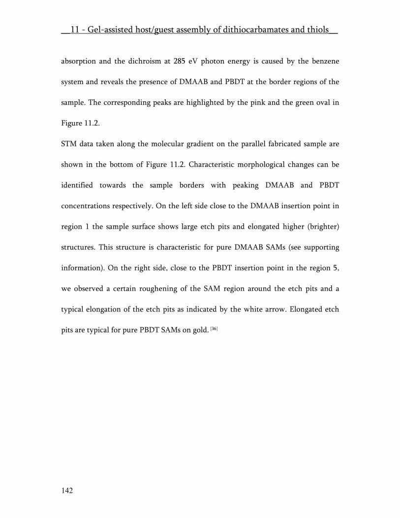
__11 - Gel-assisted host/guest assembly of dithiocarbamates and thiols__
142
absorption and the dichroism at 285 eV photon energy is caused by the benzene
system and reveals the presence of DMAAB and PBDT at the border regions of the
sample. The corresponding peaks are highlighted by the pink and the green oval in
Figure 11.2.
STM data taken along the molecular gradient on the parallel fabricated sample are
shown in the bottom of Figure 11.2. Characteristic morphological changes can be
identified towards the sample borders with peaking DMAAB and PBDT
concentrations respectively. On the left side close to the DMAAB insertion point in
region 1 the sample surface shows large etch pits and elongated higher (brighter)
structures. This structure is characteristic for pure DMAAB SAMs (see supporting
information). On the right side, close to the PBDT insertion point in the region 5,
we observed a certain roughening of the SAM region around the etch pits and a
typical elongation of the etch pits as indicated by the white arrow. Elongated etch
pits are typical for pure PBDT SAMs on gold. [36]
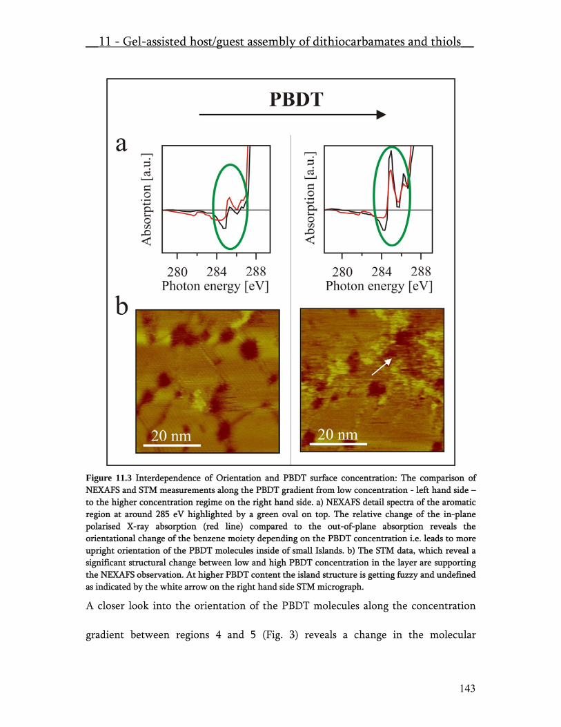
__11 - Gel-assisted host/guest assembly of dithiocarbamates and thiols__
143
Figure 11.3 Interdependence of Orientation and PBDT surface concentration: The comparison of NEXAFS and STM measurements along the PBDT gradient from low concentration - left hand side – to the higher concentration regime on the right hand side. a) NEXAFS detail spectra of the aromatic region at around 285 eV highlighted by a green oval on top. The relative change of the in-plane polarised X-ray absorption (red line) compared to the out-of-plane absorption reveals the orientational change of the benzene moiety depending on the PBDT concentration i.e. leads to more upright orientation of the PBDT molecules inside of small Islands. b) The STM data, which reveal a significant structural change between low and high PBDT concentration in the layer are supporting the NEXAFS observation. At higher PBDT content the island structure is getting fuzzy and undefined as indicated by the white arrow on the right hand side STM micrograph.
A closer look into the orientation of the PBDT molecules along the concentration
gradient between regions 4 and 5 (Fig. 3) reveals a change in the molecular
__11 - Gel-assisted host/guest assembly of dithiocarbamates and thiols__
144
orientation of PBDT. The black/red curve corresponds to the absorption of X-rays
with out-of-plane/in-plane polarisation. The change in the absorption intensity at
285 eV indicates a change in the orientation of the benzene moiety of the inserted
PBDT. The lower the concentration of the PBDT guest molecules, the more they
follow the orientation of the densely packed DT molecules. This conclusion is
further supported by the comparison of the STM data obtained in region 3 and 4,
which reveals a qualitative change from small well defined PBDT islands to larger
guest structures with fuzzy borderlines (Fig. 3).
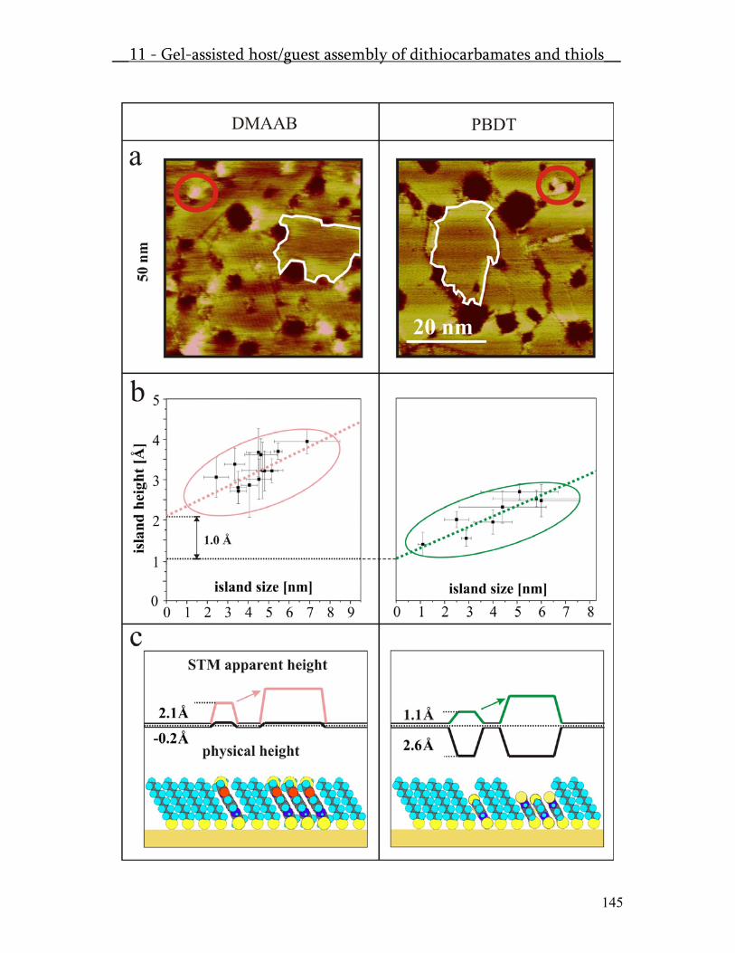
__11 - Gel-assisted host/guest assembly of dithiocarbamates and thiols__
145
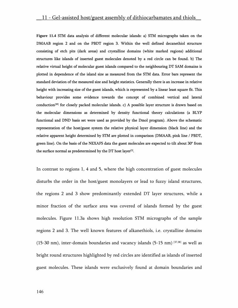
__11 - Gel-assisted host/guest assembly of dithiocarbamates and thiols__
146
Figure 11.4 STM data analysis of different molecular islands: a) STM micrographs taken on the
DMAAB region 2 and on the PBDT region 3. Within the well defined decanethiol structure
consisting of etch pits (dark areas) and crystalline domains (white marked regions) additional
structures like islands of inserted guest molecules denoted by a red circle can be found. b) The
relative virtual height of molecular guest islands compared to the neighbouring DT SAM domains is
plotted in dependence of the island size as measured from the STM data. Error bars represent the
standard deviation of the measured size and height statistics. Generally there is an increase in relative
height with increasing size of the guest islands, which is represented by a linear least square fit. This
behaviour provides some evidence towards the concept of combined vertical and lateral
conduction[39] for closely packed molecular islands. c) A possible layer structure is drawn based on
the molecular dimensions as determined by density functional theory calculations (a BLYP
functional and DND basis set were used as provided by the Dmol program). Above the schematic
representation of the host/guest system the relative physical layer dimension (black line) and the
relative apparent height determined by STM are plotted in comparison (DMAAB, pink line / PBDT,
green line). On the basis of the NEXAFS data the guest molecules are expected to tilt about 30° from
the surface normal as predetermined by the DT host layer[3].
In contrast to regions 1, 4 and 5, where the high concentration of guest molecules
disturbs the order in the host/guest monolayers or lead to fuzzy island structures,
the regions 2 and 3 show predominantly extended DT layer structures, while a
minor fraction of the surface area was covered of islands formed by the guest
molecules. Figure 11.3a shows high resolution STM micrographs of the sample
regions 2 and 3. The well known features of alkanethiols, i.e. crystalline domains
(15-30 nm), inter-domain boundaries and vacancy islands (5-15 nm) [37,38] as well as
bright round structures highlighted by red circles are identified as islands of inserted
guest molecules. These islands were exclusively found at domain boundaries and
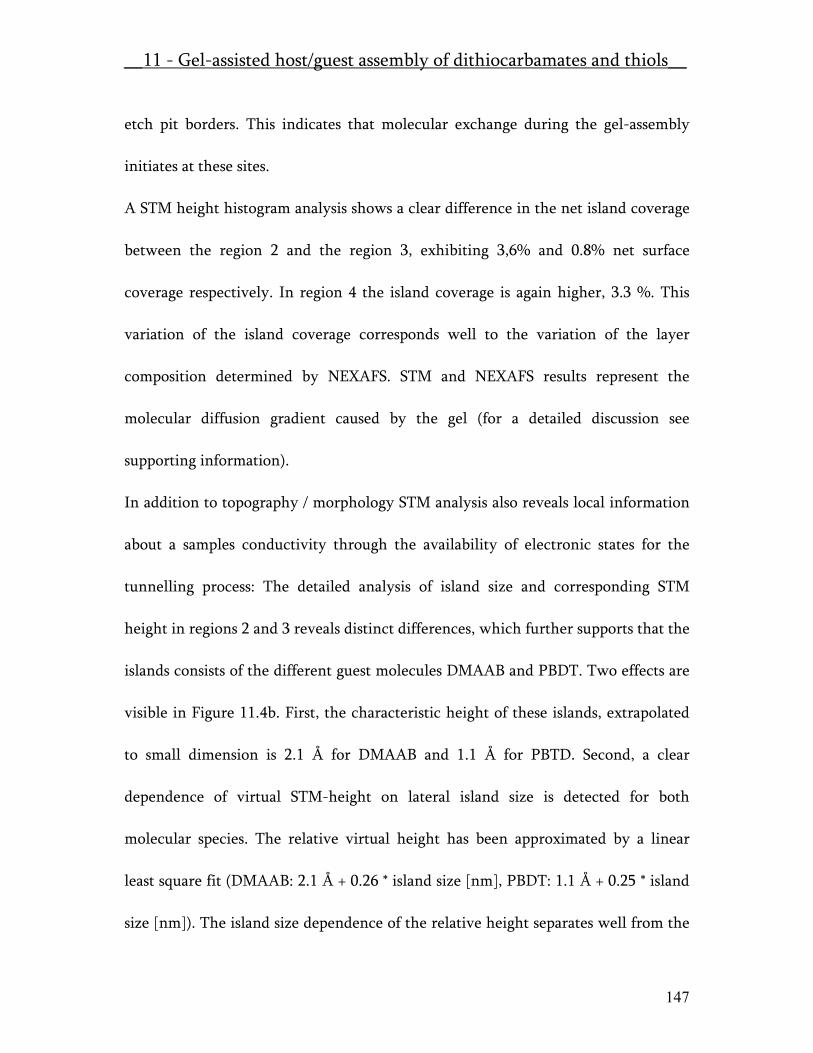
__11 - Gel-assisted host/guest assembly of dithiocarbamates and thiols__
147
etch pit borders. This indicates that molecular exchange during the gel-assembly
initiates at these sites.
A STM height histogram analysis shows a clear difference in the net island coverage
between the region 2 and the region 3, exhibiting 3,6% and 0.8% net surface
coverage respectively. In region 4 the island coverage is again higher, 3.3 %. This
variation of the island coverage corresponds well to the variation of the layer
composition determined by NEXAFS. STM and NEXAFS results represent the
molecular diffusion gradient caused by the gel (for a detailed discussion see
supporting information).
In addition to topography / morphology STM analysis also reveals local information
about a samples conductivity through the availability of electronic states for the
tunnelling process: The detailed analysis of island size and corresponding STM
height in regions 2 and 3 reveals distinct differences, which further supports that the
islands consists of the different guest molecules DMAAB and PBDT. Two effects are
visible in Figure 11.4b. First, the characteristic height of these islands, extrapolated
to small dimension is 2.1 Å for DMAAB and 1.1 Å for PBTD. Second, a clear
dependence of virtual STM-height on lateral island size is detected for both
molecular species. The relative virtual height has been approximated by a linear
least square fit (DMAAB: 2.1 Å + 0.26 * island size [nm], PBDT: 1.1 Å + 0.25 * island
size [nm]). The island size dependence of the relative height separates well from the
__11 - Gel-assisted host/guest assembly of dithiocarbamates and thiols__
148
statistical error and provides further evidence of lateral island conduction, which
has earlier been described for molecular island structures. [39] A simple 1-D model,
which includes ohmic resistors in horizontal and vertical directions to decouple the
lateral from the vertical conduction qualitatively explains the dependence of the
measured STM island height from the island size and is presented in the supporting
information. We expect that the lateral conduction originates from the
intermolecular coupling of the aromatic systems. DMAAB and PBDT both have
aromatic backbones. Therefore the latter expectation would consistently explain the
same slope observed for the island height vs. size dependence of DMAAB and PBDT.
The difference of the extrapolated height at zero island width – this value eliminates
the island vs. size dependence – is therefore a consequence of the molecular
structure i.e. the binding group.
The difference between the physical molecular height, obtained by a DFT
calculation, and the experimentally obtained STM height has been determined for
DMAAB (1.9 Å) and for PBDT (3.7 Å). Hence, there is a difference of 1.8 Å of PBDT
appearing higher compared to DMAAB, which we consequently attribute to the
difference of the electron coupling between the thiol-gold and the dithocarbamate-
gold system. [40]

__11 - Gel-assisted host/guest assembly of dithiocarbamates and thiols__
149
In summary, we have shown that the gel-assisted host/guest assembly is providing
mixed SAM systems with new and outstanding properties. These layers are
especially interesting for multi-component experiments on single molecular
conductivity, molecular switching or inelastic tunnelling spectroscopy
measurements. As exemplified in our study a number of molecular species bearing
different chemical linkers can be assembled in one layer and can reliably be
identified due to the surface gradient. Furthermore we have demonstrated the
powerful combination of NEXAFS and STM for structural investigations on SAMs.
In combination of these two techniques, SAM layers can be characterised for their
molecular composition, their molecular orientation as well as for the surface-layer
morphology. Finally we compare dithiocarbamates and thiols with respect to their
electron transport abilities and find on one hand clear evidence for lateral benzene-
coupling contributing to the total electron transport and on the other hand that
dithiocarbamates show enhanced vertical electron transport properties. This clearly
motivates further investigations and exploitations in the context of molecular
electronics applications.
Experimental Materials: Ethanol, DMF (crown capped) and NaOH were used as provided by Fluka
in p.a. quality. Water was purified using a MilliQ-system (Millipore Biocel). Low

__11 - Gel-assisted host/guest assembly of dithiocarbamates and thiols__
150
electro endo-osmosis (LE) agarose, decanethiol (DT) (≥95%) and pentanol (≥99%)
were obtained from Sigma-Aldrich and used without further purification. 1,4-
phenylene-bis-(dithiocarbamate) sodium salt (PBDT) and 1,4-
bis(mercaptoacetamido)benzene (DMAAB) were synthesised at the Sony Materials
Science Laboratory.
Au(111) film preparation: Epitaxial Au(111) films exhibiting extended terraces were
produced by sublimation of 120-150 nm gold onto freshly cleaved mica samples held
at 340 °C. Subsequently the Au film was heated up to 540°C for 5-10min. and was
allowed to cool in two steps: 5min. at 500°C, 5min. at 450°C before re-equilibration
to room temperature. This annealing procedure reproducibly lead to uniform
surfaces exhibiting characteristic triangular (111) terraces typically 200 x 200 nm2 in
size.
SAM preparation: DT SAM layers were assembled by exposure of the evaporated
gold substrate to 1mM solutions in ethanol for 18-24h. In order to get fully packed
layers the SAMs were annealed for 4h in pentanol at 45°C. For all investigations the
same substrate quality and assembly procedures were applied.
Gel-Assembly: The gel-assembly process is sketched in Figure 11.1. The annealed
thiol SAM covering flat Au(111) substrates, were put into an agarose gel (1.70g
__11 - Gel-assisted host/guest assembly of dithiocarbamates and thiols__
151
agarose put into 50ml DMF and 50ml Water, stirring and heating up to 95°C, until
the solution appears slightly opaque). During the gel exposure of the sample the gel
solution temperature must be kept below 50°C in order to prevent desintegration of
the preformed SAM. Upon cooling to room temperature, the solution transforms
into a stiff gel. Later on, two channels are dug into the gel and the molecular
solutions are filled in. After 24h of diffusive expansion (Diffusive expansion ~ 1 cm
per day, see Supporting Information) and consequent substitution into the host
layer, the gel block is reversed and the mica-gold-SAM sample is removed.
Typically, the gel removes easily from the substrate surface and samples are rinsed
with DMF and Ethanol and dried in N2-flow before the transfer to the STM and the
XMCD (SIM-beamline, SLS) chambers respectively.
NEXAFS-experiment: NEXAFS experiments were performed at the Surface/Interface
Microscopy (SIM) beamline of the Swiss Light Source, Paul Scherrer Institute. The
spectral resolution at 300 eV is around 60 meV (resolving power 1/5000) and the
linear polarization degree is 98%. The orientation of the linearly polarized X-rays
can be varied between 0 and 90 degree enabling the measurement of orientation
effects without the need to rotate the sample. The NEXAFS spectra were taken with
the total electron yield (TEY) detection, which is ideally suited for the measurement
of thin films due to the small electron escape depth of typically less than a few nm.
__11 - Gel-assisted host/guest assembly of dithiocarbamates and thiols__
152
The samples were mounted in a vacuum chamber, which was not at the focus point
of the beamline resulting in a spot size of approximately (0.5 * 0.5) mm2. The TEY
[28] signal was obtained by measuring the sample photocurrent with a
picoamperemeter and normalizing it to the intensity of the incident photon beam as
measured by the photocurrent of the Pt coating of the last mirror. In this way
information about the composition of the film is obtained, since for example the
benzene π* excitation occurs at energies of 285.0 eV[41,42] and excitations related to
the alkyl chain at 287.5 eV (mixed Rydbergstates) and 293.0 eV (C-C σ* excitation)
respectively[43] In order to determine orientation of the monolayers one has to
employ X-ray linear dichroism. Therefore, the sample surface normal was tilted by
an angle of 70° to the incident beam. Using vertically linearly polarized light one
probes the in-plane orientation whereas horizontally linearly polarized light probes
the out-of-plane components. The dichroism is then calculated XLD° = (TEYin-plane° –
TEYout-of-plane°)/(TEYin-plane° + TEYout-of-plane°). The integral of the absolute value of the
dichroism signal between 286.2 eV and 296 eV was taken as a relative measure for
the average orientation of the aliphatic chains in the SAMs.
STM-experiments: STM measurements were carried out at ambient conditions using
a Nanoscope III Multimode low current STM. Tunnelling current and bias potential
where kept at 2 pA and 100 mV. These parameters were used to prevent layer
__11 - Gel-assisted host/guest assembly of dithiocarbamates and thiols__
153
decomposition, what has been detected at higher potentials. Mechanically
sharpened Pt/Ir wire tips (0.25 mm diam.) were used for all STM experiments
reported here.
Acknowledgement
This work was financially supported by Sony Deutschland GmbH – Materials
Science Laboratory. T.J. acknowledges financial contributions from the Swiss
National Science Foundation and the NCCR Nanosciences. Part of this work was
performed at the SLS, Paul Scherrer Institut, Villigen, Switzerland.
______________________________________________________________________ [1] Nuzzo, R.G. and Allara, D.L. J. Am. Chem. Soc. 105 (1983) 4481. [2] Nuzzo, R.G.; Zegarski, B.R. and Dubois, L.H. J. Am. Chem. Soc. 109 (1987) 733. [3] Ulman, A. An Introduction to Ultrathin Organic Films: From Langmuir Blodgett to Self-Assembly; Academic Press: New York, 1991. [4] Ulman, A. Chem. Rev. 96 (1996) 1533. [5] Schreiber, F. Prog. Surf. Sci. 65 (2000) 151. [6] Love, J.C.; Estroff, L.A.; Kriebel, J.K.; Nuzzo, R.G. and Whitesides, G.M. Chem. Rev. 105 (2005) 1103. [7] Kumar, A. and Whitesides, G.M. Appl. Phys. Lett. 63 (1993) 2002. [8] Xia, Y.; Mrksich, M.; Kim, E. and Whitesides, G.M. J. Am. Chem. Soc. 117 (1995) 9576. [9] Piner, R.D.; Zhu, J.; Xu, F.; Hong, S. and Mirkin, C.A. Science 283 (1999) 661. [10] Ginger, D.S.; Zhang, H. and Mirkin, C.A. Angew. Chem. Int. Ed. 43 (2003) 30. [11] Xu, S. and Liu, G-Y. Langmuir 13 (1997) 127. [12] Amro, N.A.; Xu, S. and Liu, G-Y. Langmuir 16 (2000) 3006. [13] Lehn, J.-M. Angew. Chem. Int. Ed. Engl. 27 (1988) 89. [14] Böhringer, M.; Morgenstern, K.; Schneider, W.-D.; Berndt, R.; Mauri, F.; De Vita, A. and Car, R. Phys. Rev. Lett. 83 (1999) 324. [15] De Feyter, S. and De Schryver, F.C.; Chem. Soc. Rev. 32 (2003) 139. [16] De Wild, M.; Berner, S.; Suzuki, H.; Yanagi, H.; Schlettwein, D.; Stanislav, I.; Baratoff, A.; Gütherodt, H.-J. and Jung, T.A. ChemPhysChem 10 (2002) 881.
__11 - Gel-assisted host/guest assembly of dithiocarbamates and thiols__
154
[17] Smith, R.K.; Penelope, A.L and Weiss, P.S. Prog. Surf. Sci. 75 (2004) 1. [18] Liedberg, B. and Tengvall, P. Langmuir 11 (1995) 3821. [19] Liedberg, B.; Wirde, M.; Tao, Y-T.; Tengvall, P. and Gelius, U. Langmuir 13 (1997) 5329. [20] Lestelius, M.; Enquist, I.; Tenvall, P.; Chaudhury, M.K. and Liedberg, B. Colloids and Surfaces B: Biointerfaces 15 (1999) 57. [21] Riepl, M.; Östblom, M.; Lundström, I.; Svensson, S.C.T.; van der Gon, A.W.D.; Schäferling, M. and Liedberg, B. Langmuir 21 (2005) 1042. [22] Cui, X.D.; Primak, A.; Zarate, X.; Tomfohr, J.; Sankey, O.F.; Moore, A.L.; Moore, T.A.; Gust, D.; Harris, G. and Lindsay, S.M. Science 294 (2001) 571. [23] Cygan, M. T.; Dunbar, T. D.; Arnold, J. J.; Bumm, L. A.; Shedlock, N. F.; Burgin, T. P.; Jones, L., II; Allara, D. L.; Tour, J. M. and Weiss, P. S. J. Am. Chem. Soc. 120 (1998) 2721. [24] Donhauser, Z.J.; Mantooth, B.A.; Kelly, K.F.; Bumm, L.A.; Monnell, J.D.; Stapleton, J.J.; Price Jr. D.W.; Rawlett, A.M.; Allara, D.L.; Tour, J.M. and Weiss, P.S. Science 292 (2001) 2303. [25] Ramachandran, G.K; Hopson, T.J.; Rawlett, A.M.; Nagahara, L.A; Primak, A. and Lindsey, S.M. Science 300 (2003) 1413. [26] Stranick, S.J.; Parikh, A.N.; Tao, Y.-T.; Allara, D.L. and Weiss, P.S. J. Phys. Chem. 98 (1994) 7636. [27] Takami, H.; Delamarche, E.; Michel, B.; Gerber, Ch.; Wolf, H. and Ringsdorf, H. Langmuir 11 (1995) 3876. [28] Stöhr, J. NEXAFS Spectroscopy, Springer Series in Surface Science 25, Springer-Verlag, Berlin, Second Printing 2003. [29] Outka, D.A.; Stöhr, J.; Rabe, J.P.; Swalen, J.D. and Rotermund, H.H. Phys. Rev. Lett. 59 (1987) 1321. [30] Outka, D.A.; Stöhr, J.; Rabe, J.P. and Swalen, J.D. J. Chem. Phys. 88 (1988) 4076. [31] Hähner, G.; Wöll, Ch.; Buck, M. and Grunze, M. Langmuir 9 (1993) 1955. [32] Stöhr, J. and Outka, D.A. Phys. Rev. B 36 (1987) 7891. [33] Bain, C. and Whitesides, G.M. J. Am. Chem. Soc. 110 (1988) 3665. [34] Stöhr, J. and Outka, D.A. Phys. Rev. B 36 (1987) 7891. [35] Hähner, G.; Kinzler, M.; Thümmler, C.; Wöll, Ch. and Grunze, M. J. Vac. Sci. Technol. 10 (1992) 2758. [36] Morf, P.; Raimondi, F.; Nothofer, H.-G.; Schnyder, B.; Yasuda, A.; Wessels, J.M. and Jung, T.A. Langmuir 22 (2006) 658. [37] Schönenberger, C.; Sondag-Huethorst, J.A.M.; Jorritsma, J. and Fokkink, L.G.J. Langmuir 10 (1994) 611. [38] Schönenberger, C.; Jorritsma, J.; Sondag-Huethorst, J.A.M. and Fokkink, L.G.J. J. Phys. Chem. 99 (1995) 3259.
__11 - Gel-assisted host/guest assembly of dithiocarbamates and thiols__
155
[39] Ishida, T.; Mizutani, W.; Akiba, U.; Umemura, K.; Inoue, A.; Choi, N.; Fujihira, M. and Tokumoto, H. J. Phys. Chem. B 103 (1999) 1686. [40] Wessels, J.M.; Nothofer. H-G.; Ford, W.E.; von Wrochem, F.; Scholz, F.; Vossmeyer, T.; Schroedter, A.; Weller, H.; Yasuda, Akio. J. Am. Chem. Soc. 126 (2004) 3349. [41] Stöhr, J. and Outka, D.A. Phys. Rev. B 36 (1987) 7891. [42] Rong, H-T.; Frey, S.; Yang, Y-J.; Zharnikov, M.; Buck, M.; Wühn, M.; Wöll, Ch. And Helmchen, G. Langmuir 17 (2001) 1582. [43] Bagus, P.S.; Weiss, K.; Schertel, A.; Wöll, Ch.; Braun, W.; Hellwig, C. and Jung, C. Chem. Phys. Lett. 248 (1996) 129.

__11 - Gel-assisted host/guest assembly of dithiocarbamates and thiols__
156
11.1 Supporting Information Diffusive expansion of molecular compounds
Adsorption of thiols on gold out of solution is a very fast process. To obtain molecular gradients on surfaces one possibility is to inhibit the fast adsorption by controlling diffusion in the assembly process. To demonstrate fundamentals of diffusion it is calculated for a liquid containing tube (x: 1cm, 1-D problem). Diffusion is described by the Fick laws:
1. dtdn =
dxdcqD ⋅⋅−
2. ⎟⎠⎞
⎜⎝⎛∂∂
tc = ⎟⎟
⎠
⎞⎜⎜⎝
⎛∂∂
⋅ 2
2
xcD
⇒ c(x,t) = ( )[ ]ξψ−120c with ( ) ∫ −=
ξ
πξψ
0
22 due u and Dt
x2
=ξ
Diffusion coefficients[1] (D) of gases in different liquids, strong electrolytes in water and weak electrolytes in water are in the range of (0.4-16.4) x 10-5 cm2/s For decanethiol disolved in ethanol/DMF the diffusion coefficient was extrapolated from tabulated values of structurally similar systems: 1.5 x 10⁻⁵ cm/s. Using the values given for the error function as listed below, we can compute the diffusion rate.
Error function ( ( )ξψ ) = ( ) ∫ −=ξ
πξψ
0
22 due u ,
From Abramowitz[2]: ( ) 995.00.2 =ψ , ( ) 915.00.1 =ψ , ( ) 842.05.0 =ψ , ( ) 112.01.0 =ψ
⇒ After 1.2 h 0.5% of the initial molecular quantity reached 1 cm. After 18.5 h 8.5% has reached 1cm and After 3 d 16% has covered the distance of 1cm. ⇒ For the 3D problem, the decay of the molecular concentration is higher and we can estimate the diffusion expansion from the above. We obtain a diffusion expansion of about 1cm / day.
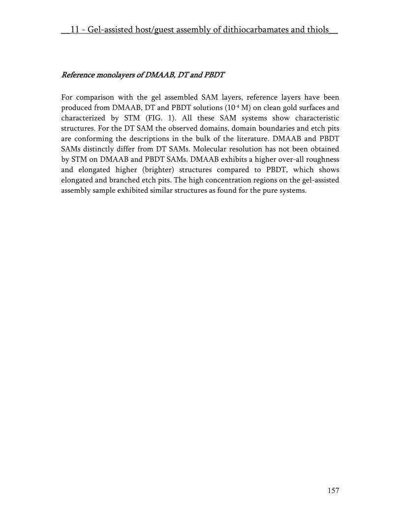
__11 - Gel-assisted host/guest assembly of dithiocarbamates and thiols__
157
Reference monolayers of DMAAB, DT and PBDT For comparison with the gel assembled SAM layers, reference layers have been produced from DMAAB, DT and PBDT solutions (10-4 M) on clean gold surfaces and characterized by STM (FIG. 1). All these SAM systems show characteristic structures. For the DT SAM the observed domains, domain boundaries and etch pits are conforming the descriptions in the bulk of the literature. DMAAB and PBDT SAMs distinctly differ from DT SAMs. Molecular resolution has not been obtained by STM on DMAAB and PBDT SAMs. DMAAB exhibits a higher over-all roughness and elongated higher (brighter) structures compared to PBDT, which shows elongated and branched etch pits. The high concentration regions on the gel-assisted assembly sample exhibited similar structures as found for the pure systems.
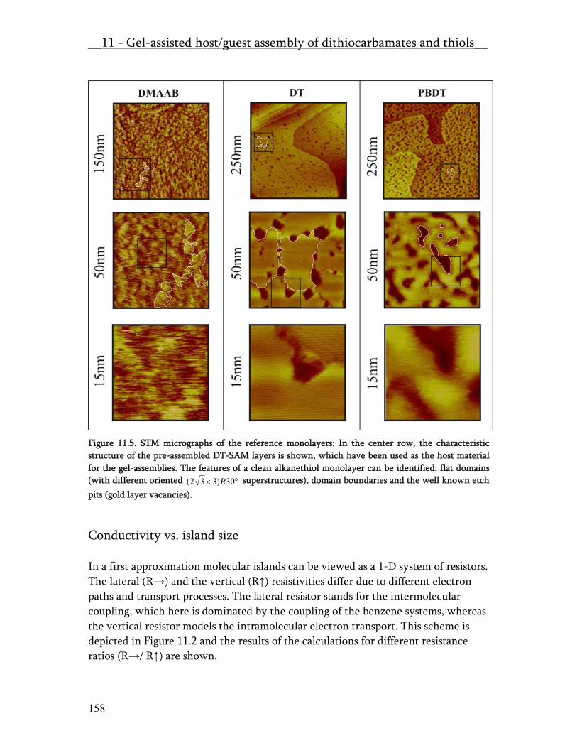
__11 - Gel-assisted host/guest assembly of dithiocarbamates and thiols__
158
Figure 11.5. STM micrographs of the reference monolayers: In the center row, the characteristic structure of the pre-assembled DT-SAM layers is shown, which have been used as the host material for the gel-assemblies. The features of a clean alkanethiol monolayer can be identified: flat domains (with different oriented °× 30)332( R superstructures), domain boundaries and the well known etch pits (gold layer vacancies).
Conductivity vs. island size In a first approximation molecular islands can be viewed as a 1-D system of resistors. The lateral (R→) and the vertical (R↑) resistivities differ due to different electron paths and transport processes. The lateral resistor stands for the intermolecular coupling, which here is dominated by the coupling of the benzene systems, whereas the vertical resistor models the intramolecular electron transport. This scheme is depicted in Figure 11.2 and the results of the calculations for different resistance ratios (R→/ R↑) are shown.
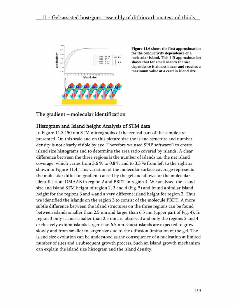
__11 - Gel-assisted host/guest assembly of dithiocarbamates and thiols__
159
The gradient – molecular identification
Histogram and Island height Analysis of STM data In Figure 11.3 150 nm STM micrographs of the central part of the sample are presented. On this scale and on this picture size the island structure and number density is not clearly visible by eye. Therefore we used SPIP software[3] to create island size histograms and to determine the area ratio covered by islands. A clear difference between the three regions is the number of islands i.e. the net island coverage, which varies from 3.6 % to 0.8 % and to 3.3 % from left to the right as shown in Figure 11.4. This variation of the molecular surface coverage represents the molecular diffusion gradient caused by the gel and allows for the molecular identification: DMAAB in region 2 and PBDT in region 4. We analysed the island size and island STM height of region 2, 3 and 4 (Fig. 5) and found a similar island height for the regions 3 and 4 and a very different island height for region 2. Thus we identified the islands on the region 3 to consist of the molecule PBDT. A more subtle difference between the island structures on the three regions can be found between islands smaller than 2.5 nm and larger than 6.5 nm (upper part of Fig. 4). In region 3 only islands smaller than 2.5 nm are observed and only the regions 2 and 4 exclusively exhibit islands larger than 6.5 nm. Guest islands are expected to grow slowly and from smaller to larger size due to the diffusion limitation of the gel. The island size evolution can be understood as the consequence of a nucleation at limited number of sites and a subsequent growth process. Such an island growth mechanism can explain the island size histogram and the island density.
Figure 11.6 shows the first approximation for the conductivity dependence of a molecular island. This 1-D approximation shows that for small islands the size dependence is almost linear and reaches a maximum value at a certain island size.
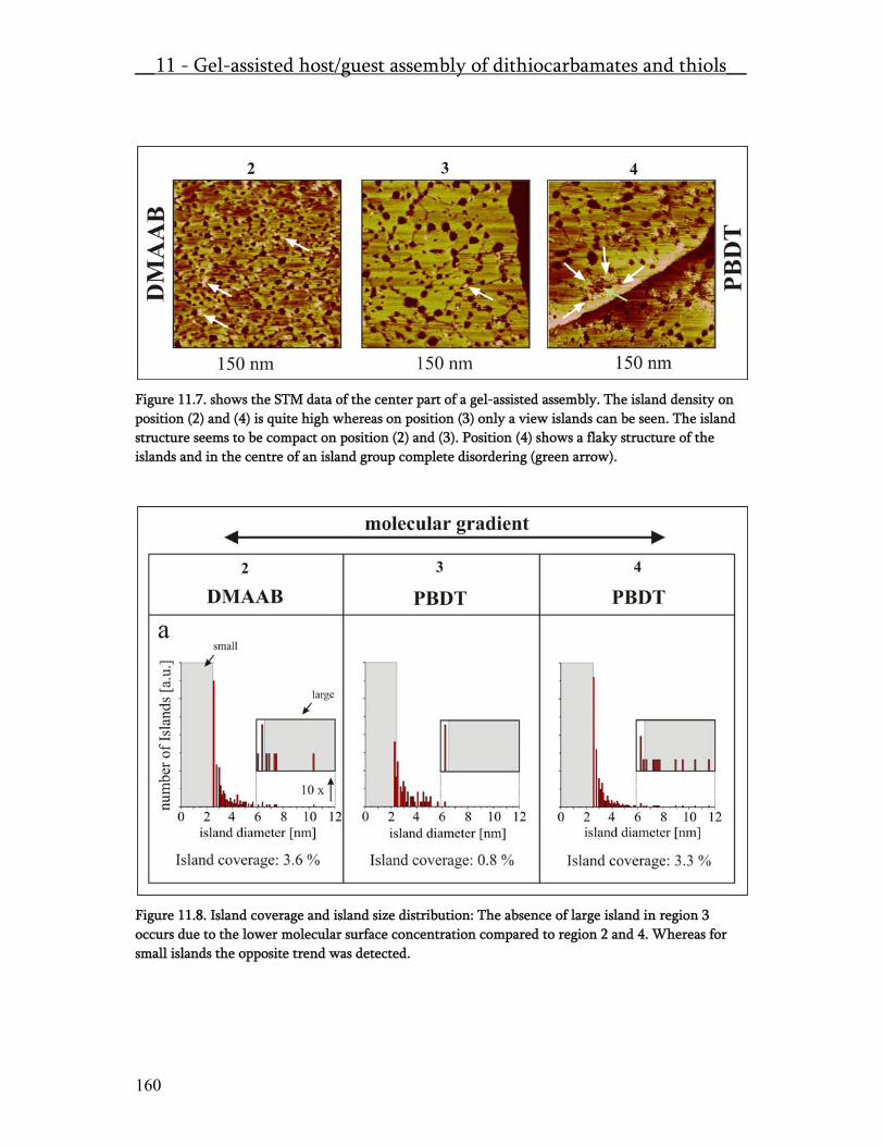
__11 - Gel-assisted host/guest assembly of dithiocarbamates and thiols__
160
Figure 11.7. shows the STM data of the center part of a gel-assisted assembly. The island density on position (2) and (4) is quite high whereas on position (3) only a view islands can be seen. The island structure seems to be compact on position (2) and (3). Position (4) shows a flaky structure of the islands and in the centre of an island group complete disordering (green arrow).
Figure 11.8. Island coverage and island size distribution: The absence of large island in region 3 occurs due to the lower molecular surface concentration compared to region 2 and 4. Whereas for small islands the opposite trend was detected.

__11 - Gel-assisted host/guest assembly of dithiocarbamates and thiols__
161
Figure 11.9. shows the analysis of the apparent STM height vs. size dependence. The regions of well ordered islands (region 2 and 3) show almost no overlap and can therefore be identified to consist of different molecules. Region 3 and 4 show almost a perfect overlap and must therefore be identified to consist of the same molecular structure. The islands in Region 4 consists of PBT thus region 3 consists of PBDT islands as well.
Molecular Size derived from Dmol calculation
Figure 11.10. shows the Dmol determination of the molecular dimensions (tilted by 30°) of DMAAB on the left hand side, PBDT in the centre part and DT on the right hand side.
______________________________________________________________________ [1] Weast, R.C. and Astle, M.J. Handbook of Chemistry and Physics 60th edition 1979-1980 CRC Press, Florida 1979. [2] Abromowitz, M. and Stegun, I.A. Handbook of Mathematical Functions. Dover 1970. [3] www.imagemet.com

162
163
12 Publications Peter Morf, Fabio Raimondi, Heinz-Georg Nothofer, Bernhard Schnyder, Akio Yasuda, Jurina M. Wessels and Thomas A. Jung. Dithiocarbamates: functional and versatile linkers for the formation of self-assembled monolayers. Langmuir 22 (2006) 658. Peter Morf. Conference Report on the “1st International Workshop on „Electrical Functionality in Nanoarchitectures”, small, issue 4 (2006) 450. Invited Publikation. Peter Morf, Fabio Raimondi, Heinz-Georg Nothofer, Bernhard Schnyder, Akio Yasuda, Jurina M. Wessels and Thomas A. Jung. Dithiocarbamates: functional and versatile linkers for the formation of self-assembled monolayers. In PSI highlights 2006. Peter Morf, Magali Vuaroqueaux, Jurina M. Wessels and Thomas A. Jung. Supramolecular surface assembly of dithiocarbamates on Au(111): Chiral trimeric domains and amorphous structures. Submitted. Peter Morf, Frithjof Nolting, Florian von Wrochem, Akos Schreiber, Heinz-Georg Nothofer, Akio Yasuda, Jurina M. Wessels and Thomas A. Jung. Co-assembly – concentration and mixing dependent ordering:Orientation and 2D ordering investigated by NEXAFS and STM. In Preparation. Peter Morf, Frithjof Nolting, Florian von Wrochem, Heinz-Georg Nothofer, Akio Yasuda, Jurina M. Wessels and Thomas A. Jung. Self-assembled host/guest gradients of bisdithiocarbamates and dithiols:Molecular distribution, orientation and conductivity in ternary assemblies. Submitted. Florian von Wrochem, Frank Scholz, Akos Schreiber, Heinz-Georg Nothofer, William E. Ford, Peter Morf, Thomas Jung, Akio Yasuda, Jurina M. Wessels. Structure and Conductance of Aromatic and Aliphatic Dithio-bisamide Monolayers on Au(111). In Preparation

______________________12 - Publications________________________
164
Oral presentations (invited contributed) Peter Morf, Florian Wrochen, Heinz-Georg Nothofer, Thomas Jung and Jurina Wessels. Physical and Chemical Mechanisms in the Organisation of Self-Assembled Monolayers (SAMs) containing different Sulphur compounds. 28th August 2003, NCCR Nanotechnology, Zurzach. Peter Morf, Florian Wrochen, Heinz-Georg Nothofer, Thomas Jung and Jurina Wessels. Physical and Chemical Mechanisms in the Organisation of Self Assembled Monolayers (SAMs) containing different Sulphur compounds. 17th February 2004, NCCR Nanotechnology, ETH – Hönggerberg. Peter Morf, Frithjof Nolting, Florian Wrochen, Heinz-Georg Nothofer, Thomas Jung and Jurina Wessels. Preparation and Characterisation of Self Assembled Monolayers (SAMs) containing different Sulphur compounds. 12th November 2004, SONS Meeting at the University of Basel. Peter Morf, Florian von Wrochen, Frithjof Nolting, Heinz-Georg Nothofer, Fabio Raimondi, Bernhard Schnyder, Akos Schreiber, Thomas A. Jung and Jurina M. Wessels. Dithiocarbamates: functional and versatile linker group for molecular electronics. Invited presentation at the, 1st International Workshop on „Electrical Functionality in Nanoarchitectures“, 24th – 25th November 2005, Rolduc Abbey, Kerkrade, The Netherlands. Jurina M. Wessels, Florian von Wrochem, Peter Morf, Heinz-Georg Nothofer, Frank Scholz, William E. Ford. Thomas A. Jung and Akio Yasuda. Dithiocarbamates: A promissing metal binding group for molecular electronic devices. 8th European Conference on Molecular Electronics 29th June- 2nd July, 2005, Bologna, Italy. Jurina M. Wessels, Florian von Wrochem, Peter Morf, Heinz-Georg Nothofer, Frank Scholz, William E. Ford. Thomas A. Jung and Akio Yasuda. Dithiocarbamates: A promissing metal binding group for molecular electronic devices. Invited presentation, ECCOER conference, Winterthur, Switzerland. Sept 28th, 2005.
______________________12 - Publications________________________
165
Jurina M. Wessels, Florian von Wrochem, Peter Morf, Heinz-Georg Nothofer, Frank Scholz, William E. Ford. Thomas A. Jung and Akio Yasuda. Dithiocarbamates: A promissing metal binding group for molecular electronic devices. Invited presentation. 2005 MRS Fall Meeting, November 28 – December 2, Boston, USA. Peter Morf, Florian von Wrochen, Frithjof Nolting, Heinz-Georg Nothofer, Fabio Raimondi, Bernhard Schnyder, Akos Schreiber, Thomas A. Jung and Jurina M. Wessels. Dithiocarbamates: functional and versatile linker group for molecular electronics. 2006 MRS Spring Meeting, April 14 – April 24, San Francisco, USA. Peter Morf, Florian von Wrochen, Frithjof Nolting, Heinz-Georg Nothofer, Fabio Raimondi, Bernhard Schnyder, Akos Schreiber, Thomas A. Jung and Jurina M. Wessels. Dithiocarbamates: functional and versatile linker group for molecular electronics. 2006 ICNT July 30 – August 4, Basel, Switzerland.
Posters Peter Morf, Florian von Wrochen, Heinz-Georg Nothofer, Frithjof Nolting, Thomas Jung and Jurina Wessels. Structure Dependent Conductivity of Thiol and Dithiol Derived Guest Host Systems. NCCR Workshop in Pontresina September 2002 Peter Morf, Florian von Wrochen, Heinz-Georg Nothofer, Frithjof Nolting, Thomas Jung and Jurina Wessels. Structure Dependent Conductivity of Thiol and Dithiol Derived Guest Host Systems. NCCR Review Panel Site Visit at the University of Basel 2003.
Peter Morf, Florian von Wrochen, Heinz-Georg Nothofer, Frithjof Nolting, Thomas Jung and Jurina Wessels. Gel-assembly Molecular gradients on surfaces – Orientation and mixing. NCCR Nanoscale Science Annual Meeting in Gwatt (Thun): 6 and 7 October 2005.


167
13 Curriculum Vitae 1968 Born in Zurich; primary and secondary school in
Zürich.
Education
2005-2006 Post Doc position at the University of Fribourg and Paul Scherrer Institute in the Group of Prof. Albert Gossauer (University of Fribourg) and in the Group of Dr. Thomas Jung (PSI). Work in the field of supramolecular chemistry and self assembled surface systems.
2002-2005 PhD student at Paul Scherrer Insitute in the Group of Dr. Thomas Jung in strong collaboration with the Group of Dr. Jurina Wessels from the Sony Material Science Laboratories in Stuttgart. The thesis – ”Self-assembled monolayers beyond thiols: Dithiocarbamates - from pure layers to ternary systems”– was performed under supervision of Prof.Christian Schönenberger from the University of Basel.
2003 Spring School at the Research Center Julich – two weeks lectures on Nanoelectronics.
1994-2001 Study at the University of Zurich. Diplomathesis in the Group of Prof Hugo Keller under supervision of Prof. Andreas Schilling: ”Konstruktion eines Differential-Thermo- Analyse-Kalorimeters für tiefe Temperaturen”. Studies in Physics (major), Mathematics (minor), Environmental Sciences (bachelor) and Informatics (minor).
1989-1992 Matura at the Kantonale Maturitätsschule für Erwachsene. In Zurich.
1984-1987 Apprenticeship as chemical lab-assistant. In Basel at Hoffman-La Roche.

______________________13 - Curriculum Vitae___________________
168
Work and Research Experience
2005-2006 Post Doc work in Supramolecular Chemistry. Surface assembly of functional polyporphyrin molecules.
2002-2005 Thesis in the field of Molecular Nanotechnology. Besides the production of flat gold films and the molecular layer formation thereupon, many new surface analytical tools were used in this thesis, as Cyclic Voltammetry, Scanning Tunneling Microscopy, Atomic Force Microscopy, Near Edge X-Ray Absorption Fine Structure, X-Ray Photoelectron Spectroscopy, Infrared- and Raman Spectroscopy, Ellipsometry, Contact Angle Measurement, Gazing Incidence X-Ray Diffraction and Mass Spectroscopy.
2000-2001 Diploma work was performed in the field of low temperature physics. This work comprised the planning and the construction of a cryostat inset to enable differential thermal analysis at low temperature and at low sample masses. Therefore some simulation work on heat flow were done and many materials and techniques related to low temperature physics were applied.
1995-1998 Studies in Environmental Science and Practical Internship in Industry for the optimization of a waste water treatment plant. The complete chemical, biological and physical analysis was learned and applied.
1992-2001 Product development, validation of the production analytics at Dr. W. Kolb AG in Hedingen. Industrial cleaners and anti-foam reagents were developed. Validation of the analytical instruments and the processes in the process control laboratory.
1988-1991 Chemical and physical analysis and safety tests. In Zürich at the Schweizerischer Elektrotechnischer Verein (SEV).
1984-1987 Organic synthesis and analysis. In Basel at Hoffmann-La Roche. Work in the field of Carotenoids and Vitamine C synthesis.
______________________13 - Curriculum Vitae___________________
169
Teachings and Supervision 2006 Reviewing for the Journal of the American Chemical
Society and for Langmuir. 2006 Mentoring of a diploma student for a master degree of
Mechatronics at the advanced technical college Konstanz.
2003-2005 Mentoring of different summer students at PSI and
introducing them into UHV, STM, AFM, CV and NEXAFS experimental techniques.
1999-2000 General physics exercise teaching for biology students. 1996-1998 Teaching private mathematical lessons on the Matura-
level and for medical students.

171
14 Acknowledgments The realization of this thesis would not have been possible without the contribution and support of many people. First, I would like to thank very much my supervisor at the PSI, Dr. Thomas Jung. It was always interesting and inspiring to shear ideas and to discuss the problems emerging during my work. Secondly, I want to thank Dr. Jurina Wessels from the Sony Materials Science Laboratory, which initiated the collaboration of Sony and the Laboratory for Micro- and Nanotechnology at the Paul Scherrer Institute (PSI). The basic concepts and ideas for the proposal of my thesis were developed in her research group. For sharing this knowledge I am very grateful. The professional supervision and always helpful support of Prof. Christian Schönenberger from the University of Basel was very important to me and my work. For his spontaneous decision to serve as an external expert to evaluate my Dissertation I am very grateful to Dr. Emanuel Delamarche from IBM. I would like to thank Marcel Mayor as well for his spontaneous assignment to act as chairman for my Dissertation Examination. As the greatest part of my work was conducted at Paul Scherrer Institute I would like to thank Jens Gobrecht the head of the Laboratory of Micro- and Nanotechnology for general support and all the technicians from LMN - Rolf Schelldorfer, Stefan Stutz, Willi Rotacher, Thomas Neiger, Anja Weber and Jana Lehmann - for their excellent assistance and lively discussions. Hans Sigg supported and encouraged me to use Infrared Spectroscopy, even though that I did not manage to get sufficient signal intensity: thank you! For in depth scientific discussions I thank very much Soichiro Tsujino and Celestino Padeste! The Students from LMN, with the one or the other I extended discussions to the Pub or Beergarden… I am very grateful to Claudio Vanoni, Philipp “Chäsr” Bernd Nöhammer, Günter Palfinger, Christian Dais, Li Zhang, Sandro Bellini, Christian Grünzweig, Andreas Scheybal, Rolf Bertschinger and the Villa inhabitants: Anna Diaz, Dirk Baches, Slawo Czekaj and especially Maxi Scheinert.

_____________________14 - Acknowledgments____________________
172
For the electrochemical coaching and the XPS measurements I thank Beat Steiger, Rüdiger Kötz, Fabio Raimondi, Bernhard Schnyder and Annette Foelske. Frihtjof Nolting offered an excellent support at the SLS, that for I am very grateful! What makes working at SLS – besides the unusual measurement time – a nice experience is due to the open and genial Scientists: Arantxa Fraile-Rodríguez, Annemieke Mulders, Phil Willmot and Bruce Patterson. As PSI is located in the middle of nowhere, the ones who traveled by train and bus became a special and colorful fellowship - Xiao Dan Li, Maria Samara, Michael Schneider, Dominik Rüegg, Sabine Streule and André Prévôt – thank you very much! To my collaborators from Sony I also would like to send many thanks. The meetings either at PSI or at Sony Stuttgart were inspiring and I very much liked the open discussions! Thanks to you Florian Von Wrochem, Heinz-Georg Nothofer and Akos Schreiber and finally – the head of the Material science Laboratory – Akio Yasuda. Apart from the scientific work I was always supported by my parents Heinrich Morf and Christine Morf-Pink and my brother Markus Morf. I would like to express my deep thankfulness for all they did to me! Additionally I want to express my gratefulness to Marie-Anne, who was my final and secure support during this work! I dedicate this thesis to my family and my wife!

173
This work has been financed by the Materials Science Laboratory, Sony Deutschland GmbH, Stuttgart, and was performed within the National Center of Competence in Research (NCCR) "Nanoscale Science".

![Acadêmico: Fabiano Bendercampeche.inf.furb.br/tccs/2012-II/TCC2012-2-10-AP-FabianoBender.p… · if self .var_flag : self .variavel[self .var_id] = [t. value , None ] return t #Método](https://static.fdocumentos.tips/doc/165x107/600087fa6805c722ae654af2/acadmico-fabiano-if-self-varflag-self-variavelself-varid-t-value.jpg)