


Línguas
Páginas
Legal

Apoio:
http://www.if.ufrj.br/~rrds/rrds.html
Esta apresentação pode ser obtida do site
seguindo o link em “Seminários, Mini-cursos, etc.”
Hole concentration vs. Mn fraction in a diluted (Ga,Mn)As ferromagnetic semiconductor
Raimundo R dos Santos (IF/UFRJ), Luiz E Oliveira (IF/UNICAMP) e
J d’Albuquerque e Castro (IF/UFRJ)

Layout
• Motivation
• Some properties of (Ga,Mn)As
• The model: hole-mediated mechanism
• New Directions
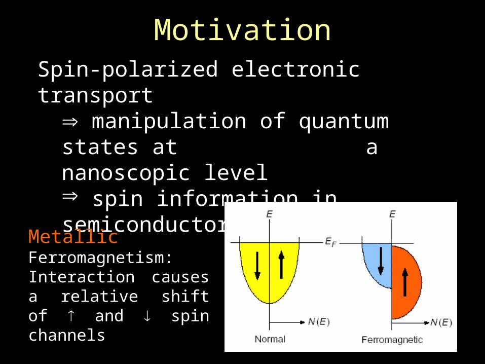
MotivationSpin-polarized electronic transport manipulation of quantum states at
a nanoscopic level spin information in semiconductors
Metallic Ferromagnetism: Interaction causes a relative shift of and spin channels

Spin-polarized device principles (metallic layers):
Parallel magnetic layers spins can flow
Antiparallel magnetic layers spins cannot flow
[Prinz, Science 282, 1660 (1998)]

Impact of spin-polarized devices:• Giant MagnetoResistance heads ( ! ) US$ 1 billion • Non-volatile memories ( ? ) US$ 100 billion
GMR RAM’s
Magnetic Tunnel Junction
Injection of spin-polarized carriers plays important role in device applications
combination of semiconductor technology with magnetism should give rise to new devices;
long spin-coherence times (~ 100 ns) have been observed in semiconductors

Magnetic semiconductors:
• Early 60’s: EuO and CdCr2S4 very hard to grow
• Mid-80’s: Diluted Magnetic Semiconductors II-VI (e.g., CdTe and ZnS) II Mn difficult to dope direct Mn-Mn AFM exchange interaction
PM, AFM, or SG (spin glass) behaviour present-day techniques: doping has led to FM for T < 2KIV-VI (e.g., PbSnTe) IV Mn hard to prepare (bulk and heterostructures) but helped understand the mechanism of carrier-mediated FM
• Late 80’s: MBE uniform (In,Mn)As films on GaAs substrates: FM on p-type.• Late 90’s: MBE uniform (Ga,Mn)As films on GaAs substrates: FM; heterostructures
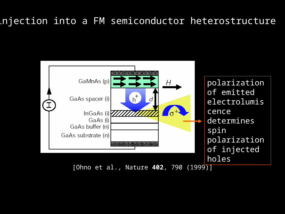
Spin injection into a FM semiconductor heterostructure
[Ohno et al., Nature 402, 790 (1999)]
polarization of emitted electrolumiscence determines spin polarization of injected holes

Some properties of (Ga,Mn)As
Ga: [Ar] 3d10 4s2 4p1
Mn: [Ar] 3d5 4s2
Photoemission Mn-induced hole states have 4p character associated with host semiconductor valence bands
EPR and optical expt’s Mn2+ has local moment S = 5/2
[For reviews on experimental data see, e.g., Ohno and Matsukura, SSC 117, 179 (2001); Ohno, JMMM 200, 110 (1999)]
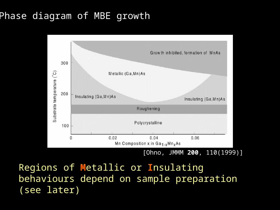
Phase diagram of MBE growth
Regions of Metallic or Insulating behaviours depend on sample preparation (see later)
[Ohno, JMMM 200, 110(1999)]

Open symbols: B in-plane• hysteresis FM with easy axis in plane; • remanence vs. T Tc ~ 60 K
x = 0.035
x = 0.053
Tc ~ 110 K
[Ohno, JMMM 200, 110(1999)]
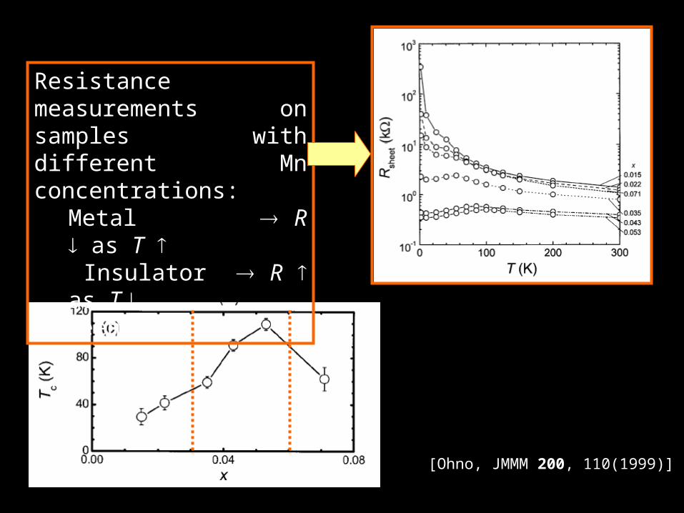
Resistance measurements on samples with different Mn concentrations:
Metal R as T Insulator R as T
Reentrant MIT
[Ohno, JMMM 200, 110(1999)]

Question: what is the hole concentration, p?
Difficult to measure since RHall dominated by the magnetic contribution; negative magnetoresistance (R as B )
Typically, one has p ~ 0.15 – 0.30 c , where c = 4 x/ a0
3, with a0 being the AsGa lattice parameter• only one reliable measurement: x = 0.053 3.5 x 1020 cm-3
Defects are likely candidates to explain difference between p and c:• Antisite defects: As occupying Ga sites• Mn complexes with As
Our purpose here: to obtain a phenomenological relation p(x) from the magnetic properties

The model: hole-mediated mechanism
= Mn, S =5/2
= hole, S =1/2 (itinerant)
Interaction between hole spin and Mn local moment is AFM, giving rise to an effective FM coupling between Mn spins
[Dietl et al., PRB 55, R3347 (1997)]
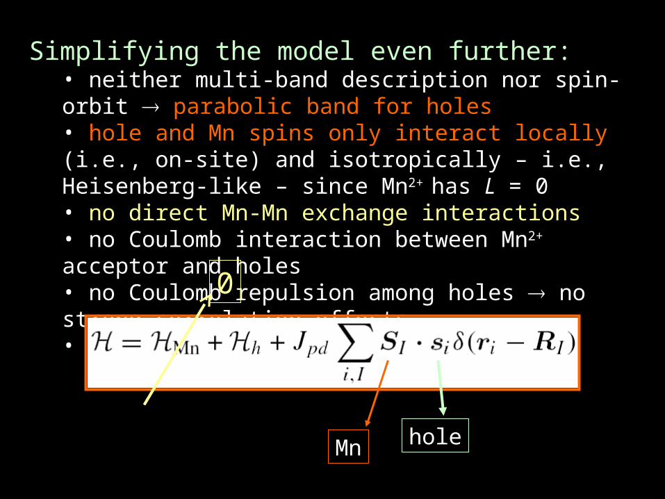
Simplifying the model even further:• neither multi-band description nor spin-orbit parabolic band for holes• hole and Mn spins only interact locally (i.e., on-site) and isotropically – i.e., Heisenberg-like – since Mn2+ has L = 0• no direct Mn-Mn exchange interactions• no Coulomb interaction between Mn2+ acceptor and holes• no Coulomb repulsion among holes no strong correlation effects• ... 0
Mn hole
1,2*2 kkk
22
h
m
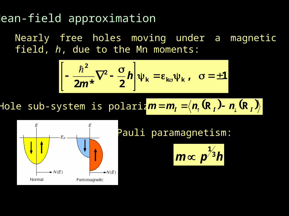
Mean-field approximation
Nearly free holes moving under a magnetic field, h, due to the Mn moments:
Hole sub-system is polarized: III nnmm RR
Pauli paramagnetism:
hpm 31

Now, the field h is related to the Mn magnetization, M :
McJMJh pdII
Ipd RRr
Assuming a uniformMn magnetization
Mn concentration
We then have
31pxMJAm pd
A depends on m* and on several constants

The Mn local moments also feel the polarization of the holes:
m
Tk
SJSBgngnM pd
SB
BMnBMn 2M
Brillouin function
Linearizing for M 0, provides the self-consistency condition to obtain Tc:
31pxMJAm pd

Now, there are considerable uncertainties in the experimental determination of m* and on Jpd [e.g., 55 10 to 15040 meV nm3].
But, within this MFA, these quantities appear in a specific combination,
2* pdJm
which can then be fitted by experimental data.
Setting S = 5/2, we can write an expression for p(x):

In most approaches x (c or n) and p are treated as independent parameters
[Schliemann et al., PRB 64, 165201 (2001)]
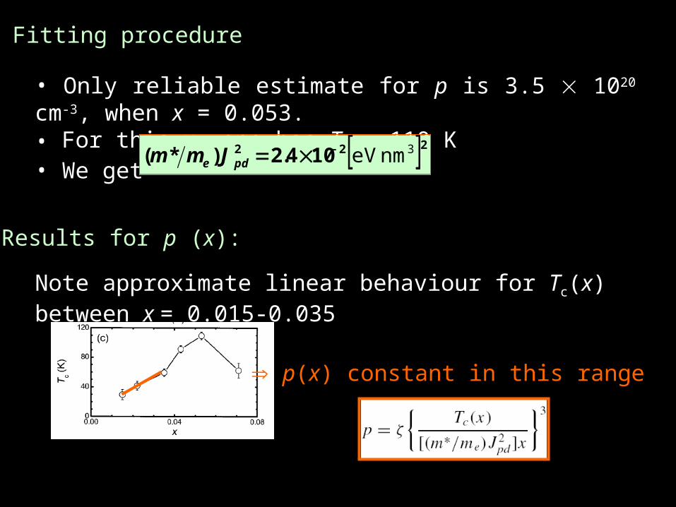
• Only reliable estimate for p is 3.5 1020 cm-3, when x = 0.053. • For this x, one has Tc = 110 K• We get
Fitting procedure
222 104.2)*( 3nmeVpde Jmm
Results for p (x):
Note approximate linear behaviour for Tc(x) between x = 0.015-0.035
p(x) constant in this range

We then get
1h/MnNotice maximum of p(x) within the M phase correlate with MIT
Early predictions
[Matsukura et al., PRB 57, R2037 (1999)]
log!
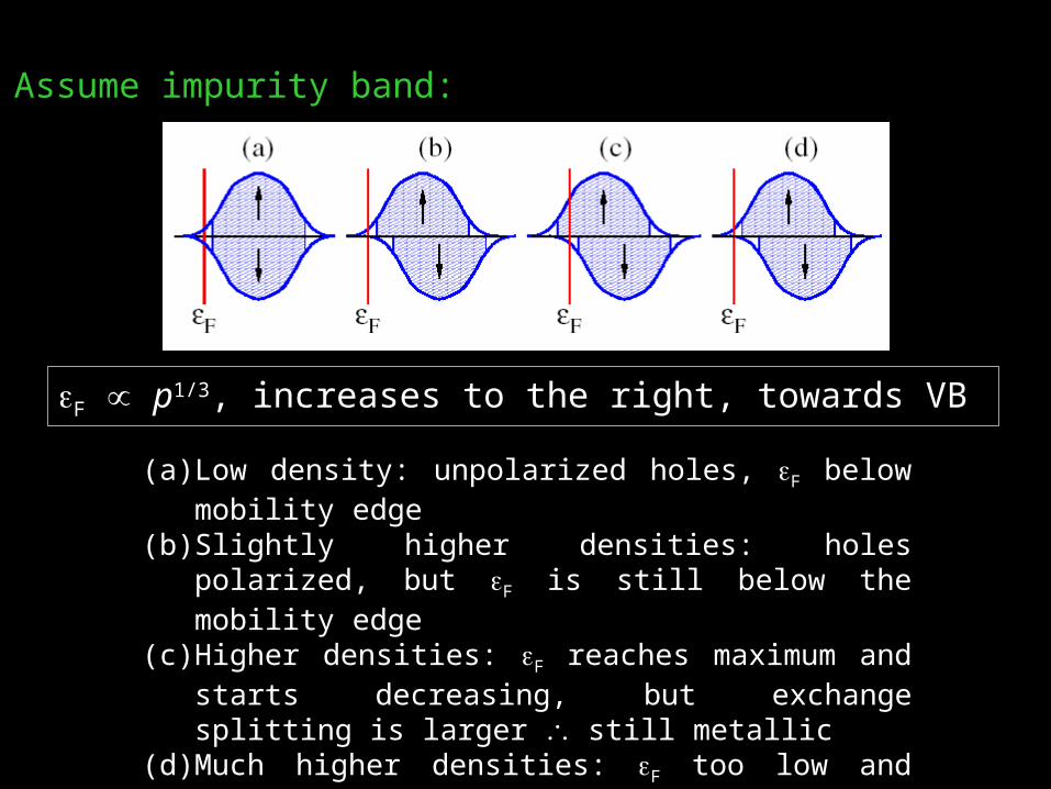
Assume impurity band:
(a) Low density: unpolarized holes, F below mobility edge(b) Slightly higher densities: holes polarized, but F is still below
the mobility edge(c) Higher densities: F reaches maximum and starts decreasing,
but exchange splitting is larger still metallic (d) Much higher densities: F too low and exchange splitting too
small F returns to localized region
F p1/3, increases to the right, towards VB

Picture supported by recent photoemission studies
[Asklund et al., cond-mat/0112287]
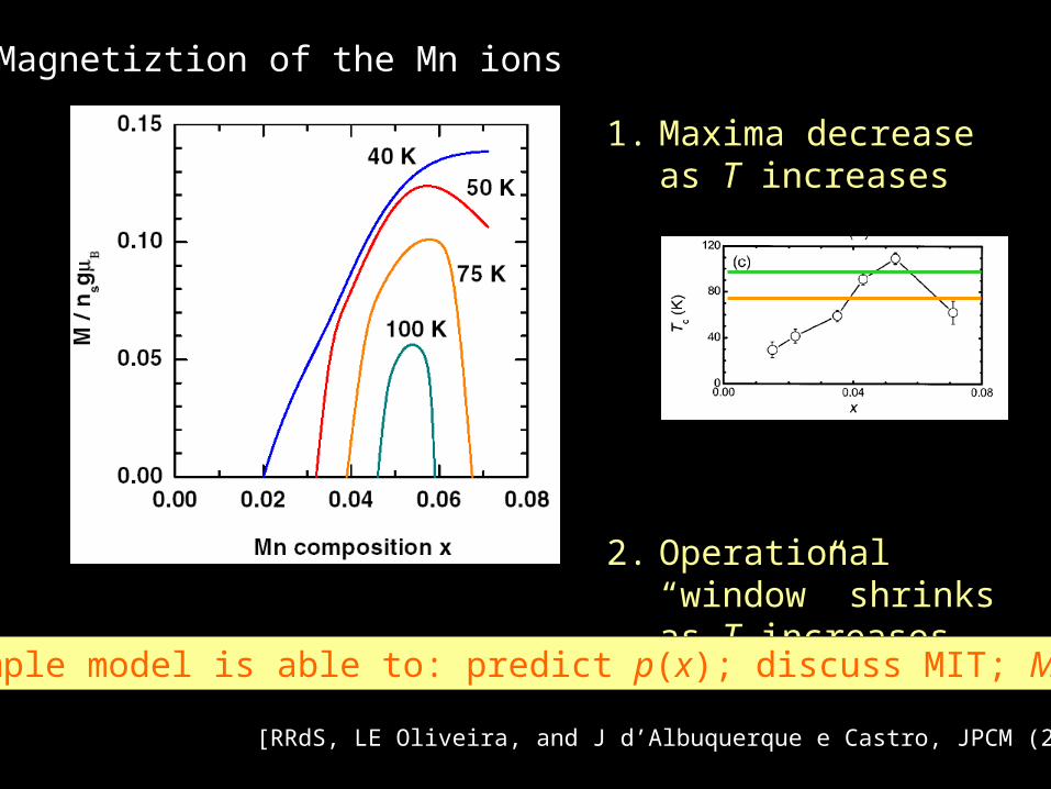
Magnetiztion of the Mn ions
1. Maxima decrease as T increases
2. Operational “window” shrinks as T increases
Simple model is able to: predict p(x); discuss MIT; M(x)
[RRdS, LE Oliveira, and J d’Albuquerque e Castro, JPCM (2002)]

New directions
I. New Materials/Geometries/Processes1. Heterostructures
(Ga,Mn)As/(Al,Ga)As/(Ga,Mn)As spin-dependent scattering, interlayer coupling, and tunnelling magnetoresistance
2. (InyGa1-y)1-x MnxAs has Tc ~ 120 K, apparently without decrease as x increases
3. (Ga,Mn) N has Tc ~ 1000 K !!!!!4. Effects of annealing time on (Ga,Mn)As

Tc grows with annealing time, up to 2hrs; for longer times, Tc decreases M as T 0 only follows T 3/2 (usual spin wave excit’ns) for annealing times longer than 30min
250 oC annealing
All samples show metallic behaviour below Tc
xx decreases with annealing time,
up to 2 hrs, and then increases again
[Potashnik et al., APL (2001)]

Two different regimes of annealing times (~2 hrs):• FM enhanced• Metallicity enhanced• lattice constant suppressed changes in defect structure:
• As antisites and correlation with Mn positions?• Mn-As complexes?
More work needed to ellucidate nature of defects and their relation to magnetic properties

II. Improvements on the model/approximations1. Give up uniform Mn approximation
averaging over disorder configurations (e.g., Monte Carlo simulations)
2. More realistic band structures3. Incorporation of defect structures4. Correlation effects in the hole sub-system
[for a review on theory see, e.g., Konig et al., cond-mat/0111314]
Top Related