
GESEP – Gerência de Especialistas em Sistemas Elétricos de ... · II. MODELING AND CONTROL...
8
GESEP – Gerência de Especialistas em Sistemas Elétricos de Potência Título: Modeling and control of a flexible photovoltaic array simulator Autores: CUPERTINO, ALLAN F. ; SANTOS, GUILHERME V. ; PEREIRA, HEVERTON A. ; SILVA, SELENIO R. ; MENDES, VICTOR F. Publicado em: 2015 IEEE 24th International Symposium on Industrial Electronics (ISIE) Data da publicação: 2015 Citação para a versão publicada: CUPERTINO, ALLAN F. ; SANTOS, GUILHERME V. ; PEREIRA, HEVERTON A. ; SILVA, SELENIO R. ; MENDES, VICTOR F. . Modeling and control of a flexible photovoltaic array simulator. In: 2015 IEEE 24th International Symposium on Industrial Electronics (ISIE), 2015, Buzios. 2015 IEEE 24th International Symposium on Industrial Electronics (ISIE), 2015. p. 318.
Transcript of GESEP – Gerência de Especialistas em Sistemas Elétricos de ... · II. MODELING AND CONTROL...

GESEP – Gerência de Especialistas em Sistemas Elétricos de Potência
Título:
Modeling and control of a flexible photovoltaic array simulator
Autores:
CUPERTINO, ALLAN F. ; SANTOS, GUILHERME V. ; PEREIRA, HEVERTON A. ; SILVA, SELENIO R. ; MENDES,
VICTOR F.
Publicado em:
2015 IEEE 24th International Symposium on Industrial Electronics (ISIE)
Data da publicação:
2015
Citação para a versão publicada:
CUPERTINO, ALLAN F. ; SANTOS, GUILHERME V. ; PEREIRA, HEVERTON A. ; SILVA, SELENIO R. ; MENDES,
VICTOR F. . Modeling and control of a flexible photovoltaic array simulator. In: 2015 IEEE 24th
International Symposium on Industrial Electronics (ISIE), 2015, Buzios. 2015 IEEE 24th International
Symposium on Industrial Electronics (ISIE), 2015. p. 318.

Modeling and Control of a Flexible Photovoltaic
Array Simulator
Allan F. Cupertino∗†, Guilherme V. Santos†, Heverton A. Pereira∗‡, Selenio R. Silva∗,Victor F. Mendes∗,∗ Graduate Program in Electrical Engineering, Federal University of Minas Gerais
Av. Antonio Carlos 6627, 31270-901, Belo Horizonte, MG, Brazil
Emails: [email protected], [email protected], [email protected]† Department of Materials Engineering, Federal Center for Technological Education of Minas Gerais
Av. Amazonas 5253, 30421-169, Belo Horizonte, MG, Brazil
Email: [email protected]‡ Departamento de Engenharia Eletrica, Universidade Federal de Vicosa
Av. P.H. Rolfs s/n, 36570-900, Vicosa, MG, Brazil
Email: [email protected]
Abstract—Photovoltaic (PV) systems have gained prominencein the current context of distributed generation systems. Thefundamental element of a PV grid-connected systems is the powerconverter. Power converters must be tested and certified accord-ing to the international standards, before being commercialized.Therefore, a flexible equipment to test the converters is necessary.This paper presents the modeling and control structure of a solararray simulator (SAS) of 10 kW for testing power converters.The limitations of conventional structures are pointed out and animproved structure based on two converter stages is proposed.The feasibility of the proposed SAS is shown through simulationsusing the Matlab/Simulink. The simulator is tested for the systemconnected to resistive loads and to a photovoltaic converter model.The dynamical behavior is evaluated through solar irradiancevariations and partial shadowing tests. The results of the proposedstructure show flexibility and good levels of power quality.
I. INTRODUCTION
The fundamental element of grid-connected photovoltaicsystem is the power converter which injects generated powerinto the electrical grid. Power converters must be tested andcertified according to the present standards, before beingcommercialized [1].
Nowadays, some documents standardize the tests to certifypower converters for photovoltaic applications. The oldestdocument is the standard of International ElectrotechnicalCommission (IEC) [2]. IEC 61683 describes different method-ologies to test the efficiency of inverters and minimum require-ments of the data acquisition equipments.
The documents elaborated by International Energy Agency[3] and Sandia National Laboratories [4] define methodologiesto test maximum power tracker accuracy, safety criteria, anti-islanding protection, etc. The Brazilian certification criteriais based on information of these documents. However, fewBrazilian laboratories certify devices for PV systems.
In a first approach, test of power converters for PV appli-cations consists in the connection of the device to a PV arrayexposed to solar irradiance. However, this method is unprac-tical due to dependence of weather conditions. Furthermore,the size of the solar array has to be adapt in order to test
converters of different rated power. Therefore, this approachresults in low flexibility.
In this situation, IEC 61683 suggests the use of a deviceknown as solar array simulator (SAS). This device is a powersource which reproduces I-V characteristics similar to a PVarray [2]. SAS can emulate the solar array behavior for a setof weather conditions (irradiance and temperature variations)and partial shadowing. Furthermore, this device can operatewith different power levels and it can be used to test inverterswith different rated power.
Most of commercial converters for photovoltaic applica-tions control the solar array output voltage in order to trackthe maximum power point. Since the purpose of the SAS isto reproduce the I-V characteristic of a solar array, the outputcurrent must be controlled. The current reference is calculatedaccording to the output voltage which is controlled by theconverter under test. The calculation of the current referencemay be complex due to the nonlinear behavior of solarpanels. In the literature, several methodologies are proposedto perform this calculation, as analogical based method, look-up table based method, analytical method, hybrid method andneural networks based method [5]–[10].
Generally, the SAS topologies present two stages: a rectifierstage based on diodes and a dc/dc converter. Dc/dc Buckconverter is the most employed in the literature [5]–[10]. Morecomplex topologies of dc/dc converters are presented by [11],[12]. Rectifiers based on diodes has harmonic distortion in gridcurrent and its output voltage is not controllable. Furthermore,the traditional dc/dc buck converter is not controllable withoutload. Therefore, open circuit point of solar panel is notemulated if this converter is employed [11], [12]. These areimportant limitations of traditional SAS structure.
Based on the mentioned limitations, an improved structureof the SAS is proposed in this work. The proposed structurehas two stages: first one is based on PWM voltage sourcerectifier, which controls the first dc bus voltage and guaranteeshigh power factor with low harmonic distortion, and the secondone consists in a bidirectional converter, permitting a stableoperation at point of open circuit.
YWXMQMTVWSMWUUTMROQUODSQNPP@ᄅRPQU@ieee SQX

II. MODELING AND CONTROL STRUCTURES
The proposed SAS structure is presented in Fig. 1. Thelook-up table based method is used in order to obtain the cur-rent reference [6]. In the following subsections are presentedthe SAS stages and the control strategy.
Vga Vgb Vgc
igb igciga
i r ic
vdc
vs
iL i s
PV inverterunder test
PV arraySimulator
Lb
Cb
Cdc
Lf Lf Lf
Fig. 1. Proposed structure for SAS (Devices in red color represent changesin traditional structure presented in literature).
A. Ac/dc stage
The rectifier stage of the SAS is based on a three phasePWM converter. A inductive filter is used in order to reducethe harmonic content generated by the IGBTs switching. Thedesign of this filter is presented in [13]. The classical controlstructure based on synchronous reference frame (dq) was em-ployed to control the PWM rectifier. For the system modeling,grid voltages are considered balanced and without harmoniccomponents. In this situation, the differential equations in thesynchronous reference frame dq are written as:
vd = −Rf id − Lf
diddt
+ ωnLf iq + Vd
vq = −Rf iq − Lf
diqdt
− ωnLf id + Vq
(1)
where Vd e Vq are the direct and quadrature components ofgrid voltage, vd and vq are the components of the fundamentalvoltage generated by the rectifier, id and iq are the componentsof the grid currents, Lf is the filter inductance and Rf is thefilter resistance.
Synchronization of the converter with grid voltage is basedon a Dual second order generalized integrator phase-lockedloop (DSOGI-PLL), proposed by [14]. This PLL has goodresponses for voltage unbalances and voltage harmonics.
The modulation strategy implemented is the space vectorPWM (SVPWM) technique. The control structure consistsin two cascade loops: internal loops control the direct andquadrature components of grid currents and external loopsregulate the dc bus voltage and the reactive power injectedinto the grid [15]. The control structure of PWM rectifier ispresented in Fig. 2.
The control digital implementation uses a sample timeequal to the switching frequency. Parameters of the PWMrectifier are presented in Appendix A.
+
-
+
+
+
r
SVPWMid
id*
Vd
wn qLi
DSOGI-PLL
VABC
VABC*
PI
-
+Vdc*
Vdc
ABC
dq
PI
+
-
+
-
iq
iq*
wn dLi
PI
-
+Q*
Q
PI
Fig. 2. Complete Control structure of PWM rectifier.
B. Dc/dc stage
The dc/dc stage control presents two modes:
• First one is the open-circuit control mode. It is re-sponsible to start the converter switching operationand to control the output voltage when the simulatoris unloaded (the tested converter is not operating). Inthis operation mode, voltage output reference is thesolar array open circuit voltage;
• Second one is the solar array simulator control mode.Based on the voltage imposed by the converter undertest, the current reference is obtained based on I x Vcharacteristic.
The control strategy of the dc/dc stage is shown in Fig. 3. Inthis block diagram is possible to see both operation modes: theopen-circuit control mode is based on a proportional-integral(PI) compensator. The SAS control mode is based on a look-up table of I x V curve. This method consists in the followingsteps: for given values of solar irradiance G and temperatureTc, a table with values of I-V curve is chosen. The value ofthe output voltage is interpolated in this table and the result isthe reference value of the inductor current. This interpolationis dynamic permitting the SAS to emulate [6].
PI
vs
G Tc
+-
*
PI+-
iL
PWMVoc
DDS1
S2
iL
Fig. 3. Complete control structure of dc/dc converter.
In the dc/dc converter modeling, the following points wereconsidered:
• The converter switches are driven in complementary;
• The dc bus voltage of the rectifier is constant;
• The power consumption of the inverter under test ismodeled as a resistance in parallel with a currentsource connected to the output of the solar arraysimulator.
SQY
Based on these considerations, simplified model of thedc/dc stage is presented in Fig. 4. The transfer function whichrelates inductor current and converter duty cycle is given by[16]:
ic
vdc
vs
iL i s
Lb
Cb
*
Rs
i s
i load
Fig. 4. Simplified model of dc/dc converter.
Gid(s) =(RsCb + 1)Vdc
RsLbCbs2 + (Lb +RLbRsCb)s+ (Rs +RLb).
(2)
The transfer function that relates the inductor current andthe dc bus voltage, considering solar array simulator unloaded,is given by:
Gvi(s) =1
Cbs. (3)
The current control loop is used in both control modesof the PV array simulator using PI compensator. A PI com-pensator is also used in the voltage control loop. Thesecompensators are designed by poles placement based method.Parameters of the converter are presented in Appendix. Thedigital implementation of the control uses a sample time equalto the switching frequency.
III. SIMULATION RESULTS
In this section the simulations results of the proposed PVarray simulator structure are presented and their analysis iscarried out. The parameters of simulation model are presentedin the Appendix.
The voltage control performance during the system start-up, i.e., the SAS operating unloaded is presented. After, the SAScontrol response is analyzed during variations of irradianceand partial shadowing, considering a resistive load. Finally, thesimulation results for the simulator supplying a photovoltaicconverter are discussed.
A. Proposed Start-up and open circuit voltage control
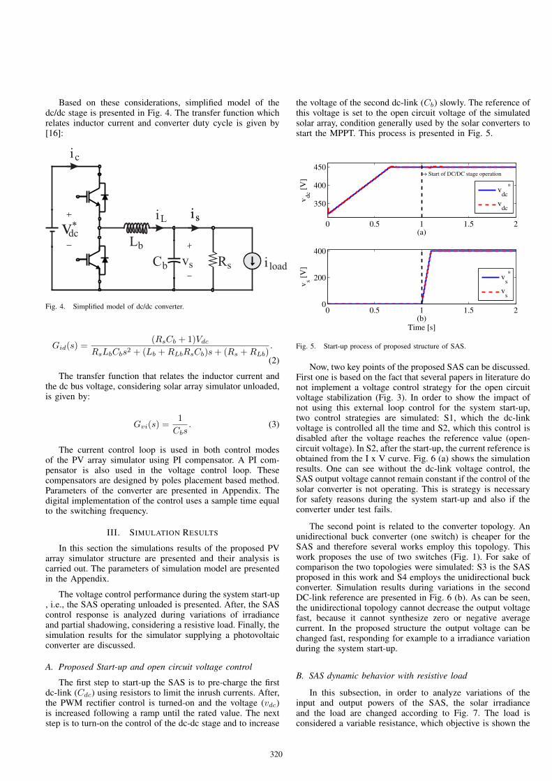
The first step to start-up the SAS is to pre-charge the firstdc-link (Cdc) using resistors to limit the inrush currents. After,the PWM rectifier control is turned-on and the voltage (vdc)is increased following a ramp until the rated value. The nextstep is to turn-on the control of the dc-dc stage and to increase
the voltage of the second dc-link (Cb) slowly. The reference ofthis voltage is set to the open circuit voltage of the simulatedsolar array, condition generally used by the solar converters tostart the MPPT. This process is presented in Fig. 5.
0 0.5 1 1.5 2
350
400
450
(a)
vd
c [V
]
→ Start of DC/DC stage operation
vdc
*
vdc
0 0.5 1 1.5 20
200
400
(b)Time [s]
vs [
V]
vs
*
vs
Fig. 5. Start-up process of proposed structure of SAS.
Now, two key points of the proposed SAS can be discussed.First one is based on the fact that several papers in literature donot implement a voltage control strategy for the open circuitvoltage stabilization (Fig. 3). In order to show the impact ofnot using this external loop control for the system start-up,two control strategies are simulated: S1, which the dc-linkvoltage is controlled all the time and S2, which this control isdisabled after the voltage reaches the reference value (open-circuit voltage). In S2, after the start-up, the current reference isobtained from the I x V curve. Fig. 6 (a) shows the simulationresults. One can see without the dc-link voltage control, theSAS output voltage cannot remain constant if the control of thesolar converter is not operating. This is strategy is necessaryfor safety reasons during the system start-up and also if theconverter under test fails.
The second point is related to the converter topology. Anunidirectional buck converter (one switch) is cheaper for theSAS and therefore several works employ this topology. Thiswork proposes the use of two switches (Fig. 1). For sake ofcomparison the two topologies were simulated: S3 is the SASproposed in this work and S4 employs the unidirectional buckconverter. Simulation results during variations in the secondDC-link reference are presented in Fig. 6 (b). As can be seen,the unidirectional topology cannot decrease the output voltagefast, because it cannot synthesize zero or negative averagecurrent. In the proposed structure the output voltage can bechanged fast, responding for example to a irradiance variationduring the system start-up.
B. SAS dynamic behavior with resistive load
In this subsection, in order to analyze variations of theinput and output powers of the SAS, the solar irradianceand the load are changed according to Fig. 7. The load isconsidered a variable resistance, which objective is shown the
SRP

0 1 2 3 40
50
100
150
200
250
300
350
400
(a)
vs [
V]
1 2 3 4390
395
400
405
410
415Detail
S1
S2
1 1.2 1.4 1.6 1.8 2 2.20
50
100
150
200
250
300
350
400
450
(b)Time [s]
vs [
V]
1 1.5 2350
400
450
Detail
S3
S4
Fig. 6. Simulation results comparing control strategies S1 and S2.
SAS operation in various points on the I-V characteristic curveemulated. At time 7 seconds, a partial shadowing is considered.
0 1 2 3 4 5 6 7 8 90
400
700
1000
Irra
dia
nce
[W
/m2]
Time [s]0 1 2 3 4 5 6 7 8 9
0
50
100
Load
Res
ista
nce
[Ω
]
Fig. 7. Simulated solar irradiance and load resistance profiles.
Fig. 8 presents the behavior of the PWM rectifier. Onecan see load variations generate disturbances in the rectifierdc-link voltage, but the voltage variations are smaller than2 % of the rated value, proving the dc-link voltage controlis adequate. Fig. 8 (b) presents the grid active and reactivepowers. The reactive power is controlled in zero, resulting ina unitary power factor.
1.5 2 2.5 3 3.5 4445
450
455
460
(a)
vd
c [V
]
vdc
*
vdc
2 3 4 5 6 7 8 9−5
0
5
10
(b)Time [s]
Pg [
kW
] an
d Q
g[k
VA
]
Pg
Qg
Fig. 8. Dynamic behavior of PWM rectifier during SAS operation withresistive load: (a) Dc bus voltage; (b) Active and reactive power supplied byelectrical grid.
Fig. 9 (a) and (b) present the behavior of dc/dc converter,showing the output current is follows the reference i∗L. Loadchanges results in change of operation point. The inductorcurrent iL presents a larger ripple which is filters by meansof output capacitor. Therefore, SAS output current presentssmaller ripple, but its dynamic behavior changes in terms ofovershoot. When non-uniform shadow starts, an overshoot isobserved in the current response.
Fig. 10 presents paths of SAS in I x V plane. Thesepaths illustrates inductor current variation which follows I x Vreference curves. System starts at point A (open circuit voltage)changes to point B (load variation with constant irradiance),C (irradiance variation with constant load), D(load variationwith constant irradiance) and finish at point E (constant irradi-ance with load variation). Transient in current response whenpartial shadowing starts results in a larger error when SASoperation point changes from D to E. However, this transientis fast and probably will not influence the MPPT algorithm ofphotovoltaic inverter.
SRQ

2 3 4 5 6 7 8 90
100
200
300
400
(a)
vs [
V]
2 3 4 5 6 7 8 9−10
0
10
20
30
40
(b)Time [s]
i L [
A]
iL
iL
*
is
Fig. 9. Dynamic behavior of dc/dc converter during SAS operation withresistive load: (a) Output voltage; (b) Inductor and output currents.
0 50 100 150 200 250 300 350 4000
5
10
15
20
25
30
35
A
E
B
C
DR = 100 Ω
R = 5 ΩG = 1000 W/m2
G = 700 W/m2
G = 400 W/m2, non−uniform
Cu
rren
t [A
]
Voltage [V]
Emulator
Reference
Fig. 10. Paths of SAS in I x V plane with resistive load.
C. SAS dynamic behavior testing a photovoltaic converter
In order to evaluate the dynamic behavior of the proposedSAS during the test of a photovoltaic converter, a boostconverter is simulated. This converter was chosen since severaltopologies of commercial photovoltaic inverters present a dc/dcboost input stage. Fig. 11 shows the boost converter and thecontrol strategy. A classical MPPT algorithm based on perturband observe is employed [17].
The irradiance profile presented in Fig. 7 is used in this
PI
Vs
IL
+-
*
PI+-
iL
PWMDD S1
Lb
Cb
iL
Vinv
Is
Vs
MPPTVs
Is
Fig. 11. Control strategy of MPPT boost converter.
simulation. The SAS output voltage (now imposed by theMPPT converter) and the output current are presented in Fig.12. These values change in terms of solar irradiance due toconverter MPPT operation. The resulting output power andP x V reference curves are presented in Fig. 13. MPPTof the converter reach point of maximum power point anddo not changes significantly the SAS dynamic behavior. Ahigher power ripple is observed for 400W/m2, because theinfluence of inductor current ripple increases when the outputcurrent reduces. Nevertheless, one can see that the SAS canemulate the array I-V curve and the tested converter reachesthe maximum power point as expected.
2 4 6 8 10 12300
320
340
360
380
400
(a)
vs [
V]
2 4 6 8 10 12 14
0
10
20
30
(b)Time [s]
i L [
A]
iL
is
iL
*
Fig. 12. SAS output voltage and current during the test of the MPPTconverter.
SRR

0 100 200 300 4000
2
4
6
8
10
G = 1000 W/m2, T
c = 25 ºC
G = 700 W/m2, T
c = 25 ºC
G = 400 W/m2, T
c = 35 ºC
Po
wer
[k
W]
Voltage [V]
Simulator
Reference
MPP
Fig. 13. Paths of SAS in P x V plane during the operation of the MPPTconverter.
IV. CONCLUSION
This work presented a topology of solar array simulatorbased on a PWM rectifier and a bidirectional dc/dc converter.The proposed control strategy stabilizes the SAS output whenit is unloaded, permitting a correct system start-up. Limitationsof unidirectional buck converter topology, used in severalworks, are pointed out.
Simulation results show that the SAS can emulate the Ix V curves of solar arrays during irradiance variations andpartial shadowing. The simulations were carried out first usinga resistive load and after testing a MPPT converter, bothdemonstrating good results.
The next step in the development is to implement theproposed strategies in a test bench in order to validate thework with experimental results.
ACKNOWLEDGMENT
The authors would like to thank CNPQ, FAPEMIG andCAPES for their assistance and financial support.
APPENDIX
Simulation parameters of dc/dc converter are presented inTable IV. Parameters of PWM rectifier are presented in TableIV.
TABLE I. DC/DC CONVERTER PARAMETERS.
Parameter Value
Pmax 10 kW
fs 10 kHz
L 5 mH
C 1 mF
RL 62.5 mΩ
TABLE II. PWM RECTIFIER PARAMETERS.
Parameter Value
Pmax 10 kW
Vg 220 V
fn 60 Hz
fs 6 kHz
Lf 4 mH
Rf 5mΩ
Cdc 3.06 mF
REFERENCES
[1] M. Camino-Villacorta, M. A. Egido-Aguilera, and P. Daz,“Test procedures for maximum power point tracking chargecontrollers characterization,” Progress in Photovoltaics: Research
and Applications, vol. 20, no. 3, pp. 310–320, 2012. [Online].Available: http://dx.doi.org/10.1002/pip.1139
[2] IEC, Photovoltaic systems Power conditioners Procedure for mea-
suring efficiency, 1st ed. International Electrotechnical Commission,November 1999.
[3] I. PVPS, International Guideline for the Certification of Photovoltaic
System Components and Grid-Connected systems, 1st ed. IEA,September 2002.
[4] SANDIA, Performance Test Protocol for Evaluating Inverters Used in
Grid-Connected Photovoltaics Systems, 1st ed. SANDIA, September2004.
[5] J. Ollila, “A medium power pv-array simulator with a robust controlstrategy,” in Control Applications, 1995., Proceedings of the 4th IEEE
Conference on, Sep 1995, pp. 40–45.
[6] H. Matsukawa, K. Koshiishi, H. Koizumi, K. Kurokawa, M. Hamadac,and L. Bo, “Dynamic evaluation of maximum power point trackingoperation with pv array simulator,” Solar Energy Materials and Solar
Cells, vol. 75, no. 3, pp. 537–546, Feb 2003.
[7] S. Gonzalez, S. Kuszmaul, D. Deuel, and R. Lucca, “Pv array simulatordevelopment and validation,” in Photovoltaic Specialists Conference
(PVSC), 2010 35th IEEE, June 2010, pp. 002 849–002 852.
[8] L. Bun, B. Raison, G. Rostaing, S. Bacha, A. Rumeau, and A. Labonne,“Development of a real time photovoltaic simulator in normal andabnormal operations,” in IECON 2011 - 37th Annual Conference on
IEEE Industrial Electronics Society, Nov 2011, pp. 867–872.
[9] Z. G. Piao, S. J. Gong, Y. H. An, and G. B. Cho, “A study onthe pv simulator using equivalent circuit model and look-up tablehybrid method,” in Electrical Machines and Systems (ICEMS), 2013
International Conference on, Oct 2013, pp. 2128–2131.
[10] M. Di Piazza, M. Pucci, A. Ragusa, and G. Vitale, “Analytical versusneural real-time simulation of a photovoltaic generator based on a dc-dcconverter,” Industry Applications, IEEE Transactions on, vol. 46, no. 6,pp. 2501–2510, Nov 2010.
[11] Z. Jike and W. Shengtie, “Design and simulation of digital pv simulatorbased on push-pull forward converter,” in Power and Energy Engineer-
ing Conference (APPEEC), 2012 Asia-Pacific, March 2012, pp. 1–5.
[12] C.-H. Chang, C. Lin, and C.-W. Ku, “A high efficiency solar arraysimulator implemented by an llc resonant dc/dc converter,” in Power
Electronics Conference (IPEC), 2010 International, June 2010, pp.2603–2609.
[13] S. Ponnaluri, V. Krishnamurthy, and V. Kanetkar, “Generalized systemdesign and analysis of pwm based power electronic converters,” inIndustry Applications Conference, 2000. Conference Record of the 2000
IEEE, vol. 3, 2000, pp. 1972–1979 vol.3.
[14] P. Rodriguez, R. Teodorescu, I. Candela, A. Timbus, M. Liserre,and F. Blaabjerg, “New positive-sequence voltage detector for gridsynchronization of power converters under faulty grid conditions,” inPower Electronics Specialists Conference, 2006. PESC ’06. 37th IEEE,June 2006, pp. 1–7.
[15] M. Liserre, F. Blaabjerg, and S. Hansen, “Design and control of anlcl-filter based three-phase active rectifier,” in Industry Applications
Conference, 2001. Thirty-Sixth IAS Annual Meeting. Conference Record
of the 2001 IEEE, vol. 1, Sept 2001, pp. 299–307 vol.1.
SRS

[16] D. M. Robert W. Erickson, Fundamentals of Power Electronics.Kluwer Academic Publishers, 2004.
[17] D. Sera, L. Mathe, T. Kerekes, S. Spataru, and R. Teodorescu, “On theperturb-and-observe and incremental conductance mppt methods for pvsystems,” Photovoltaics, IEEE Journal of, vol. 3, no. 3, pp. 1070–1078,July 2013.
SRT
pッキ・イ・、@「ケ@tcpdf@HキキキNエ」ー、ヲNッイァI