
Design and Implementation of the MorphoSys …gram.eng.uci.edu/morphosys/docs/JVSP.pdfDesign and...
29
1 Design and Implementation of the MorphoSys Reconfigurable Computing Processor Ming-Hau Lee, Hartej Singh, Guangming Lu, Nader Bagherzadeh, Fadi J. Kurdahi University of California, Irvine, USA {mlee, hsingh, glu, nader, kurdahi}@ece.uci.edu Eliseu M.C. Filho and Vladimir Castro Alves Federal University of Rio de Janeiro (Brazil) [email protected], [email protected] Abstract. In this paper, we describe the implementation of MorphoSys, a reconfigurable processing system targeted at data-parallel and computation-intensive applications. The MorphoSys architecture consists of a reconfigurable component (an array of reconfigurable cells) combined with a RISC control processor and a high bandwidth memory interface. We briefly discuss the system-level model, array architecture, and control processor. Next, we present the detailed design implementation and the various aspects of physical layout of different sub- blocks of MorphoSys. The physical layout was constrained for 100 MHz operation, with low power consumption, and was implemented using 0.35 m, four metal layer CMOS (3.3 Volts) technology. We provide simulation results for the MorphoSys architecture (based on VHDL model) for some typical data-parallel applications (video compression and automatic target recognition). The results indicate that the MorphoSys system can achieve significantly better performance for most of these applications in comparison with other systems and processors. 1. Introduction Reconfigurable computing systems are systems that consist of some reconfigurable hardware along with software programmable processors. The reconfigurable component provides the ability to configure or customize the system for one or more applications [1]. In the ideal case, a reconfigurable system delivers high performance typical of ASIC devices and also provides the flexibility of a general-purpose processor (i.e. it can execute a wide range of applications). Conventionally, field programmable gate arrays (FPGAs) [2] are the most common devices used for implementing reconfigurable components. This is because FPGAs allow designers to manipulate gate-level devices such as flip-flops, memory and other logic gates. However, FPGAs have certain disadvantages such as low logic density and inefficient performance for word-level datapath operations. Hence, many researchers have proposed
Transcript of Design and Implementation of the MorphoSys …gram.eng.uci.edu/morphosys/docs/JVSP.pdfDesign and...
1
Design and Implementation of the MorphoSys Reconfigurable
Computing ProcessorMing-Hau Lee, Hartej Singh, Guangming Lu, Nader Bagherzadeh, Fadi J. Kurdahi
University of California, Irvine, USA
{mlee, hsingh, glu, nader, kurdahi}@ece.uci.edu
Eliseu M.C. Filho and Vladimir Castro Alves
Federal University of Rio de Janeiro (Brazil )
[email protected], [email protected]
Abstract. In this paper, we describe the implementation of MorphoSys, a reconfigurable processing system
targeted at data-parallel and computation-intensive applications. The MorphoSys architecture consists of a
reconfigurable component (an array of reconfigurable cells) combined with a RISC control processor and a high
bandwidth memory interface. We briefly discuss the system-level model, array architecture, and control processor.
Next, we present the detailed design implementation and the various aspects of physical layout of different sub-
blocks of MorphoSys. The physical layout was constrained for 100 MHz operation, with low power consumption,
and was implemented using 0.35 � m, four metal layer CMOS (3.3 Volts) technology. We provide simulation results
for the MorphoSys architecture (based on VHDL model) for some typical data-parallel applications (video
compression and automatic target recognition). The results indicate that the MorphoSys system can achieve
significantly better performance for most of these applications in comparison with other systems and processors.
1. Introduction
Reconfigurable computing systems are systems that consist of some reconfigurable hardware along with
software programmable processors. The reconfigurable component provides the abili ty to configure or customize the
system for one or more applications [1]. In the ideal case, a reconfigurable system delivers high performance typical
of ASIC devices and also provides the flexibili ty of a general-purpose processor (i.e. it can execute a wide range of
applications). Conventionally, field programmable gate arrays (FPGAs) [2] are the most common devices used for
implementing reconfigurable components. This is because FPGAs allow designers to manipulate gate-level devices
such as flip-flops, memory and other logic gates. However, FPGAs have certain disadvantages such as low logic
density and inefficient performance for word-level datapath operations. Hence, many researchers have proposed
2
prototypes of reconfigurable computing systems that employ non-FPGA reconfigurable components such as DPGA
[4], Garp [5], PADDI [6], MATRIX [7], RaPiD [8], REMARC [9], and RAW [10].
In this paper, we describe the implementation of MorphoSys, which is based on a novel model of a
reconfigurable computing system. This model is aimed at applications that feature high data-parallelism, regularity,
and are computation-intensive. Some examples of these applications are video compression, graphics and image
processing, and DSP transforms. The implementation of MorphoSys operates at 100 MHz, and the entire design has
a sili con area of about 200 sq. mm.
1.1 Organization of paper
Section 2 introduces the system architecture and components of MorphoSys. A cross-section of related work is
briefly described and contrasted with MorphoSys architecture in Section 3. The physical implementation aspects of
the MorphoSys system, with its focus on clock cycle of 10 ns (for operating freq. of 100 MHz) and low power
consumption, are presented in Section 4. Section 5 gives an overview of the current programming and simulation
environment for MorphoSys. Next, in Section 6, we provide performance estimates for a set of applications (video
compression and ATR) that have been mapped to MorphoSys. Finally, we list some conclusions in Section 7.
2. MorphoSys Architecture
The MorphoSys design model incorporates a reconfigurable component (to handle high-volume data-parallel
operations), on the same die with a general-purpose RISC processor (to perform sequential processing and control
functions), and a high bandwidth memory interface.
2.1 MorphoSys Components
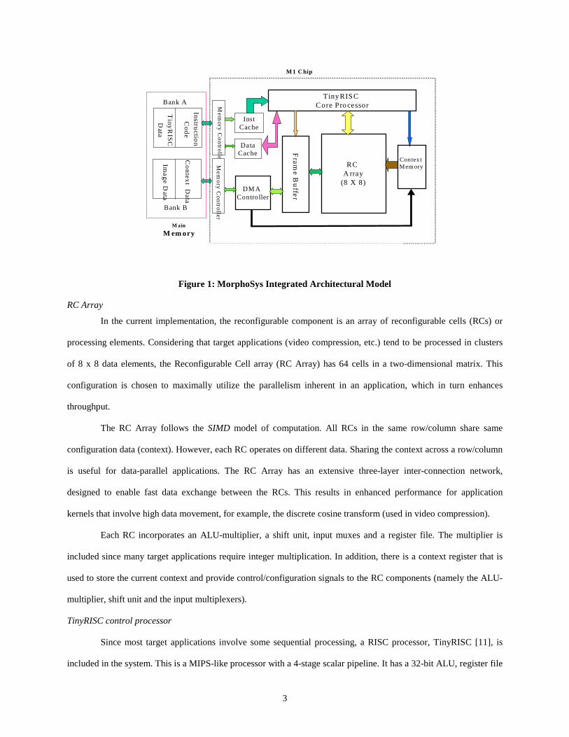
The MorphoSys architecture comprises five major components: the Reconfigurable Cell Array (RC Array),
control processor (TinyRISC), Context Memory, Frame Buffer and a DMA Controller. Figure 1 shows the
organization of the integrated MorphoSys reconfigurable computing system.
3
TinyRISC Core Processor
Context M emoryRC
A rray(8 X 8)
DM A Control ler
InstCache
DataCache
Bank A
Bank B
Instructio
n
Co
de
Tiny
RIS
C
Data
Image
Data
Mem
ory Co
ntroller
M ain
M em or y
Fram
e B
uffer
M 1 C hip
Co
ntext D
ata
Mem
ory Co
ntroller
Figure 1: MorphoSys Integrated Architectural Model
RC Array
In the current implementation, the reconfigurable component is an array of reconfigurable cells (RCs) or
processing elements. Considering that target applications (video compression, etc.) tend to be processed in clusters
of 8 x 8 data elements, the Reconfigurable Cell array (RC Array) has 64 cells in a two-dimensional matrix. This
configuration is chosen to maximally utilize the parallelism inherent in an application, which in turn enhances
throughput.
The RC Array follows the SIMD model of computation. All RCs in the same row/column share same
configuration data (context). However, each RC operates on different data. Sharing the context across a row/column
is useful for data-parallel applications. The RC Array has an extensive three-layer inter-connection network,
designed to enable fast data exchange between the RCs. This results in enhanced performance for application
kernels that involve high data movement, for example, the discrete cosine transform (used in video compression).
Each RC incorporates an ALU-multiplier, a shift unit, input muxes and a register file. The multiplier is
included since many target applications require integer multiplication. In addition, there is a context register that is
used to store the current context and provide control/configuration signals to the RC components (namely the ALU-
multiplier, shift unit and the input multiplexers).
TinyRISC control processor
Since most target applications involve some sequential processing, a RISC processor, TinyRISC [11], is
included in the system. This is a MIPS-like processor with a 4-stage scalar pipeline. It has a 32-bit ALU, register file
4
and an on-chip data cache memory. This processor also coordinates system operation and controls its interface with
the external world. This is made possible by addition of specific instructions (besides the standard RISC
instructions) to the TinyRISC ISA. These instructions initiate data transfers between main memory and MorphoSys
components, and control execution of the RC Array.
Frame Buffer and DMA Controller
The high parallelism of the RC Array would be ineffective if the memory interface is unable to transfer
data at an adequate rate. Therefore, a high-speed memory interface consisting of a streaming buffer (Frame Buffer)
and a DMA controller is incorporated in the system. The Frame Buffer has two sets, which work in complementary
fashion to enable overlap of data transfers with RC Array execution.
Context Memory
The Context Memory stores multiple (32) planes of configuration data (context) for RC Array, thus
providing depth of programmabil ity. This implies that the system spends less time loading fresh configuration data.
Fast dynamic reconfiguration is essential for achieving high performance with a reconfigurable system. MorphoSys
supports single-cycle dynamic reconfiguration (without interruption of RC Array execution).
2.2 System Control Mechanism
MorphoSys implements a novel control mechanism for the reconfigurable component through the TinyRISC
instructions. The TinyRISC ISA has been modified to include several new instructions (Table 1) that enable control
of different components in the system. These instructions contain fields that directly provide the values for different
control signals to the RC Array, DMA controller, Frame Buffer and the Context Memory. There are two major
categories of these new instructions: DMA instructions and RC Array instructions.
The DMA instructions contain fields that provide the DMA Controller with adequate information (starting address
in main memory, starting address in Frame Buffer of Context Memory, number of bytes to load, load or store
control). This enables transfer of data between main memory and the Frame Buffer or the Context Memory through
the DMA Controller.
The RC Array instructions have fields that provide the control signals to the RC Array and the Context
Memory. This is essential to enable the execution of computations in the RC Array. This information includes the
5
contexts to be executed, the mode of context broadcast (row or column), location of data to be loaded in from Frame
Buffer, etc.
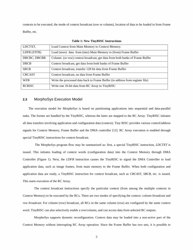
Table 1: New TinyRISC Instructions
LDCTXT, Load Context from Main Memory to Context Memory.
LDFB (STFB) Load (store) data from (into) Main Memory to (from) Frame Buffer
DBCBC, DBCBR Column (or row) context broadcast, get data from both banks of Frame Buffer
DBCB Context broadcast, get data from both banks of Frame Buffer
SBCB Context broadcast, transfer 128 bit data from Frame Buffer
CBCAST Context broadcast, no data from Frame Buffer
WFB Write the processed data back to Frame Buffer (in address from register file)
RCRISC Write one 16-bit data from RC Array to TinyRISC
2.3 MorphoSys Execution Model
The execution model for MorphoSys is based on partitioning applications into sequential and data-parallel
tasks. The former are handled by the TinyRISC, whereas the latter are mapped to the RC Array. TinyRISC initiates
all data transfers involving application and configuration data (context). Tiny RISC provides various control/address
signals for Context Memory, Frame Buffer and the DMA controller [12]. RC Array execution is enabled through
special TinyRISC instructions for context broadcast.
The MorphoSys program flow may be summarized as: first, a special TinyRISC instruction, LDCTXT is
issued. This initiates loading of context words (configuration data) into the Context Memory through DMA
Controller (Figure 1). Next, the LDFB instruction causes the TinyRISC to signal the DMA Controller to load
application data, such as image frames, from main memory to the Frame Buffer. When both configuration and
application data are ready, a TinyRISC instruction for context broadcast, such as CBCAST, SBCB, etc. is issued.
This starts execution of the RC Array.
The context broadcast instructions specify the particular context (from among the multiple contexts in
Context Memory) to be executed by the RCs. There are two modes of specifying the context: column broadcast and
row broadcast. For column (row) broadcast, all RCs in the same column (row) are configured by the same context
word. TinyRISC can also selectively enable a row/column, and can access data from selected RC outputs.
MorphoSys supports dynamic reconfiguration. Context data may be loaded into a non-active part of the
Context Memory without interrupting RC Array operation. Since the Frame Buffer has two sets, it is possible to
6
overlap computation in RC Array with data transfers between external memory and the Frame Buffer. While the RC
Array performs computations on data in one Frame Buffer set, fresh data may be loaded in the other set or the
Context Memory may receive new contexts.
3. Related Work
There are two major classes of reconfigurable systems: fine-grain (processing units have datapath widths of a
few bits) and coarse-grain (basic processing elements have data-paths of eight or sixteen bits or more). Research
prototypes with fine-grain granularity include Splash [3], DPGA [4] and Garp [5]. Reconfigurable processors with
coarse-grain granularity are PADDI [6], MATRIX [7], RaPiD [8], and REMARC [9]. MorphoSys is a coarse-grain
architecture, since the target applications mostly involve pixel-processing. In this section, we compare and contrast
some of the previously developed coarse-grain systems with MorphoSys.
Among the systems of MATRIX, PADDI, RaPiD, REMARC and RAW [10], MorphoSys has some common
features with each, as well as some differences. A major difference is that most of these designs have not been
implemented at the physical hardware level, whereas MorphoSys has been developed from the VHDL level down to
the physical layout level and will be actually fabricated.
PADDI [6] has a different mechanism for storing and broadcasting the context word, it has less depth of
programmabili ty, more complex interconnection network using crossbar switches, and a distinct VLIW flavor since
the instruction word is 53 bits. The EXUs receive the same global instruction but the decoded instruction is different
for each EXU, which is different from MorphoSys. In MorphoSys, each row (column) of RCs receives the same
context word, and it has same function for each.
MATRIX [7] has a similar interconnection network as MorphoSys, but unlike MorphoSys, the control and array
processors are configured out of the same hardware resources. This makes the dynamic system control becomes
quite complex. MATRIX lacks a multiplier in the basic processing element, the BFU. The levels of interconnect have
variable delay (in terms of pipeline stages); this is constant for MorphoSys. This work does not specify the data
interface to the external world.
RaPiD [8] is designed as a linear array of functional units, configured as a linear computation pipeline.
Therefore, it performs well for systolic applications, but has limited performance for block-oriented application
7
tasks, which MorphoSys performs very efficiently (even transpose operations are not needed). However, there is no
unified macro-controller and an integrated memory interface is missing.
REMARC [9] has 64 nano-processors but these nano-processors do not have a multiplier (even though it targets
multimedia applications), but instead have a 16 entry data RAM. The interconnection network has two levels, and
the global control unit has to perform the functions of data transfers to the main processor/memory, whereas in
MorphoSys, these transfers are carried out by the DMA controller, and are concurrent with the program execution. It
does not allow dynamic reconfiguration.
RAW [10] is a system with a set of interconnected tiles of RISC processors. The configuration time for the
interconnect switches is quite high (several instructions per switch). The design has many VLIW features, and each
tile includes a FPGA-like configurable logic. Having a large number of RISC processors seems inefficient, when we
consider that MorphoSys is able to execute several data-parallel applications at a high performance level using just
one RISC processor.
In summary, the most prominent features incorporated in the MorphoSys architecture are:
� Integrated model: This has a novel control mechanism for the reconfigurable component that uses a general-
purpose processor. Except for main memory, MorphoSys is a complete system-on-a-chip.
� Multiple contexts on-chip: this feature enables fast single-cycle reconfiguration.
� On-chip controller: allows efficient execution of applications that have both serial and parallel tasks.
� Innovative memory interface: high data throughput by using a two-set data buffer that allows overlap of
computation with data transfer.
4. Implementation and Verification
In this section, we describe the steps involved in the design and implementation of the major components of
MorphoSys: the reconfigurable cell (RC), the TinyRISC, the Context Memory, the Frame Buffer and the DMA
Controller. The chip is designed using 0.35 � m 3.3 V four metal layers CMOS technology.
Design Methodology : MorphoSys components are implemented using the twin approaches of custom
design and standard cell design. The components that constitute the critical path (e.g. RC) or the components that
have a regular structure (e.g. Context Memory, and Frame Buffer) are custom designed. This enables extensive
optimization of these components for the delay and area. The components that are control intensive, consist of
8
random logic or are not in the critical path, are designed using logic synthesis tools (Synopsys and Mentor Graphics
software). Four metal layers are available for routing; out of these, two (Metal 3 and Metal 4) are reserved for
routing between the component blocks. Only two layers are used for routing within a component (such as the
reconfigurable cell ). We use both IRSIM (switch-level simulator) and Hspice (transistor-level simulator) to verify
the design of custom components. For synthesized components, Lsim simulator (switch mode and adept mode) is
used for functional verification and timing analysis.
4.1 Reconfigurable Cell
C o nte xt M em o ry
D ata(31 .....0 )
M UX A
XQ
RM
A L U +M UL T
R E G
O utput
A LU _C T R L
Co
nte
xt R
eg
iste
r
C onstan t
A dd ress From T inyR IS C
T C B
M UX B
S H IFTA LU _S F T
R egister F ile
R 0
R 3
I U D L
RF
0R
F1
RF
2R
F3
16 (X 2)E ntries
R 1
R 2
R 3
R 2
R 1
R 0
L VE
I
FL A G
AL
U_
OP
MU
XA
MU
XB
Co
ns
tan
t
RE
G_
FIL
E
Write
_E
XP
R
RS
_L
S
11 ...031 14 ...1 218 ...1 622 ...1 926 ...2 3
AL
U_
SF
T
29 ...2 830
Write
_R
F_
En
27
H E
16
28
16
1616 8
V E H E
To _F B
W E &R ow _co l
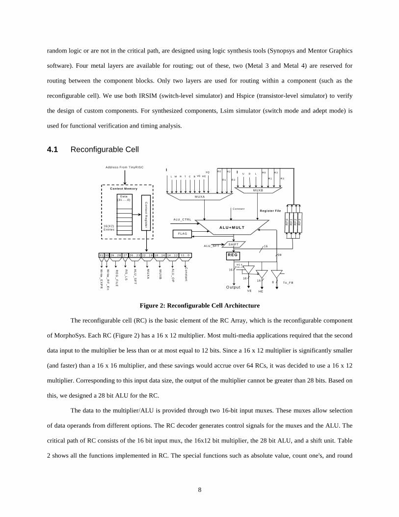
Figure 2: Reconfigurable Cell Architecture
The reconfigurable cell (RC) is the basic element of the RC Array, which is the reconfigurable component
of MorphoSys. Each RC (Figure 2) has a 16 x 12 multiplier. Most multi-media applications required that the second
data input to the multiplier be less than or at most equal to 12 bits. Since a 16 x 12 multiplier is significantly smaller
(and faster) than a 16 x 16 multiplier, and these savings would accrue over 64 RCs, it was decided to use a 16 x 12
multiplier. Corresponding to this input data size, the output of the multiplier cannot be greater than 28 bits. Based on
this, we designed a 28 bit ALU for the RC.
The data to the multiplier/ALU is provided through two 16-bit input muxes. These muxes allow selection
of data operands from different options. The RC decoder generates control signals for the muxes and the ALU. The
critical path of RC consists of the 16 bit input mux, the 16x12 bit multiplier, the 28 bit ALU, and a shift unit. Table
2 shows all the functions implemented in RC. The special functions such as absolute value, count one's, and round
9
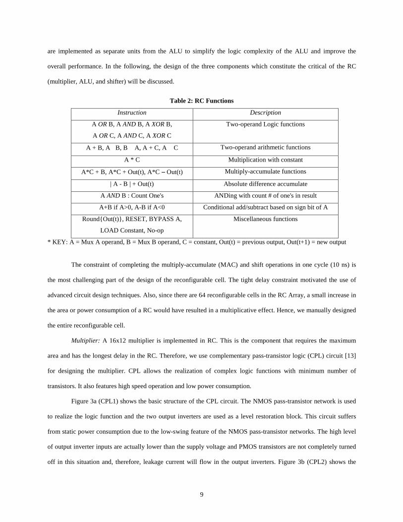
are implemented as separate units from the ALU to simplify the logic complexity of the ALU and improve the
overall performance. In the following, the design of the three components which constitute the critical of the RC
(multiplier, ALU, and shifter) will be discussed.
Table 2: RC Functions
Instruction Description
A OR B, A AND B, A XOR B,
A OR C, A AND C, A XOR C
Two-operand Logic functions
A + B, A � B, B � A, A + C, A � C Two-operand arithmetic functions
A * C Multiplication with constant
A*C + B, A*C + Out(t), A*C � Out(t) Multiply-accumulate functions
| A - B | + Out(t) Absolute difference accumulate
A AND B : Count One's ANDing with count # of one's in result
A+B if A>0, A-B if A<0 Conditional add/subtract based on sign bit of A
Round{ Out(t)} , RESET, BYPASS A,
LOAD Constant, No-op
Miscellaneous functions
* KEY: A = Mux A operand, B = Mux B operand, C = constant, Out(t) = previous output, Out(t+1) = new output
The constraint of completing the multiply-accumulate (MAC) and shift operations in one cycle (10 ns) is
the most challenging part of the design of the reconfigurable cell . The tight delay constraint motivated the use of
advanced circuit design techniques. Also, since there are 64 reconfigurable cells in the RC Array, a small increase in
the area or power consumption of a RC would have resulted in a multiplicative effect. Hence, we manuall y designed
the entire reconfigurable cell .
Multiplier: A 16x12 multiplier is implemented in RC. This is the component that requires the maximum
area and has the longest delay in the RC. Therefore, we use complementary pass-transistor logic (CPL) circuit [13]
for designing the multiplier. CPL allows the realization of complex logic functions with minimum number of
transistors. It also features high speed operation and low power consumption.
Figure 3a (CPL1) shows the basic structure of the CPL circuit. The NMOS pass-transistor network is used
to realize the logic function and the two output inverters are used as a level restoration block. This circuit suffers
from static power consumption due to the low-swing feature of the NMOS pass-transistor networks. The high level
of output inverter inputs are actually lower than the supply voltage and PMOS transistors are not completely turned
off in this situation and, therefore, leakage current will flow in the output inverters. Figure 3b (CPL2) shows the
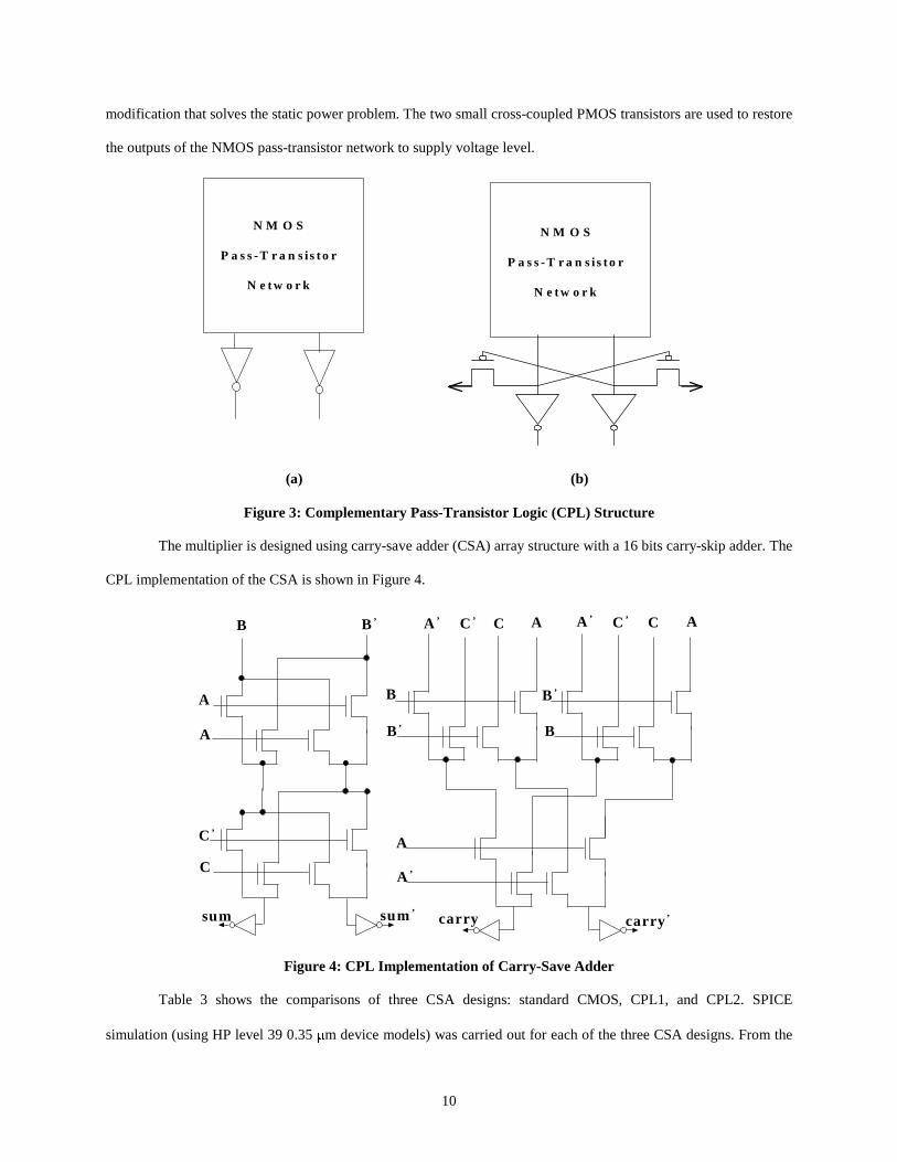
10
modification that solves the static power problem. The two small cross-coupled PMOS transistors are used to restore
the outputs of the NMOS pass-transistor network to supply voltage level.
N M O S
P a ss-T r a n si st o r
N et w o r k
N M O S
P a ss-T r a n si st o r
N et w o r k
(a) (b)
Figure 3: Complementary Pass-Transistor Logic (CPL) Structure
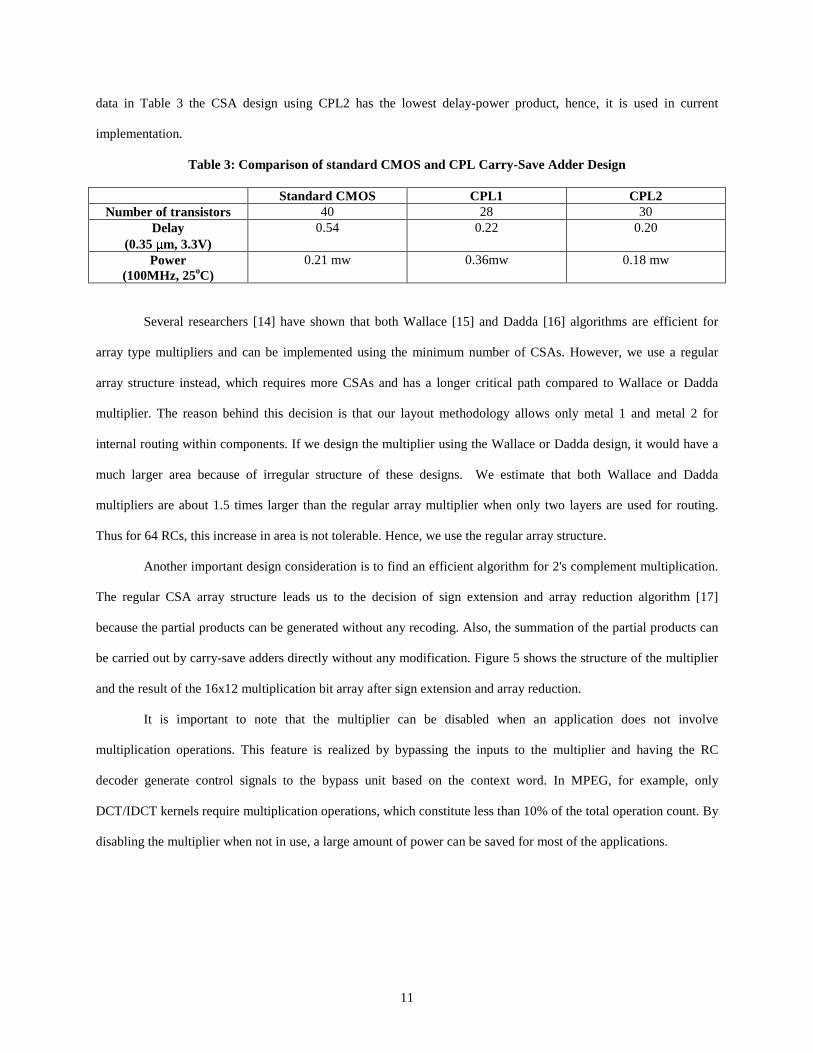
The multiplier is designed using carry-save adder (CSA) array structure with a 16 bits carry-skip adder. The
CPL implementation of the CSA is shown in Figure 4.
B B ’
A
A
C ’
C
sum sum ’
B
B ’
B ’
B
A ’ C ’ C A A ’ C ’ C A
car r y car r y ’
A
A ’
Figure 4: CPL Implementation of Carr y-Save Adder
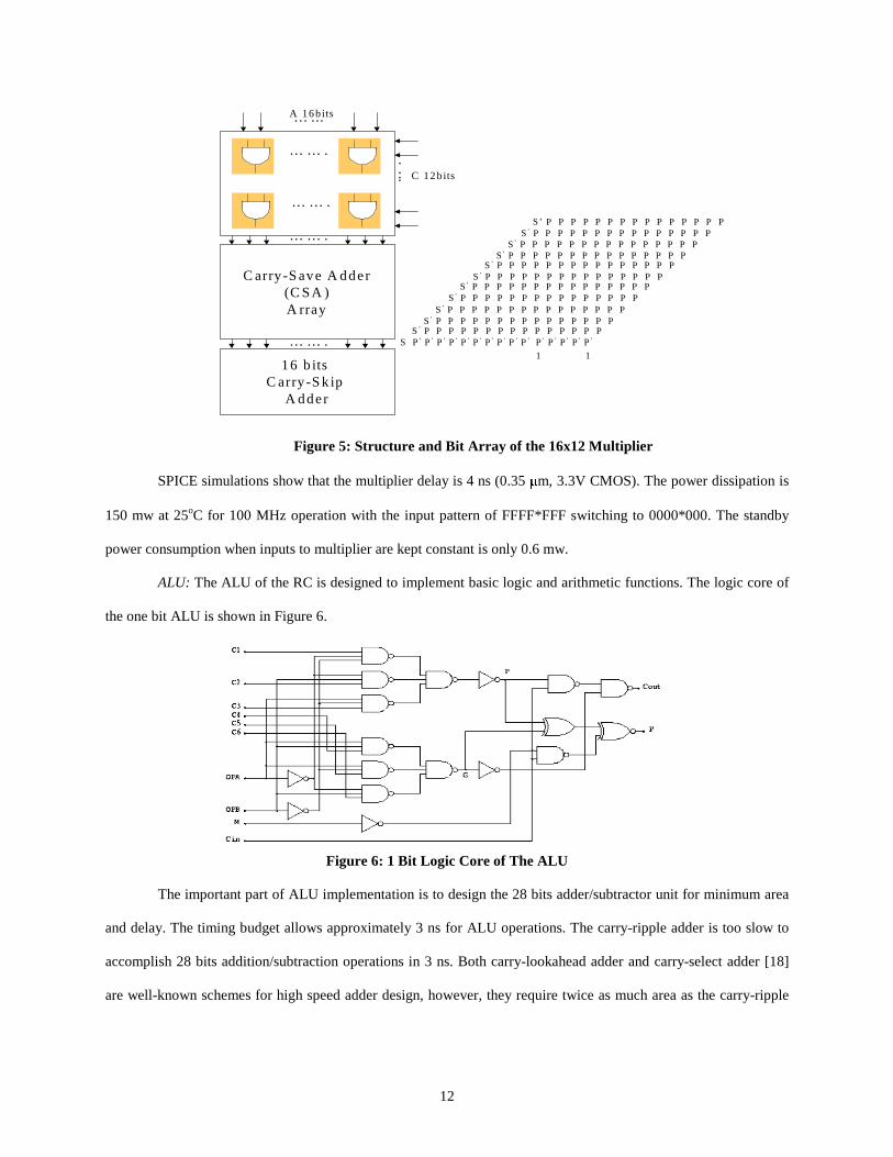
Table 3 shows the comparisons of three CSA designs: standard CMOS, CPL1, and CPL2. SPICE
simulation (using HP level 39 0.35 � m device models) was carried out for each of the three CSA designs. From the
11
data in Table 3 the CSA design using CPL2 has the lowest delay-power product, hence, it is used in current
implementation.
Table 3: Compar ison of standard CMOS and CPL Carr y-Save Adder Design
Standard CMOS CPL1 CPL2Number of transistors 40 28 30
Delay(0.35 � � m, 3.3V)
0.54 0.22 0.20
Power(100MHz, 25oC)
0.21 mw 0.36mw 0.18 mw
Several researchers [14] have shown that both Wallace [15] and Dadda [16] algorithms are efficient for
array type multipliers and can be implemented using the minimum number of CSAs. However, we use a regular
array structure instead, which requires more CSAs and has a longer critical path compared to Wallace or Dadda
multiplier. The reason behind this decision is that our layout methodology allows only metal 1 and metal 2 for
internal routing within components. If we design the multiplier using the Wallace or Dadda design, it would have a
much larger area because of irregular structure of these designs. We estimate that both Wallace and Dadda
multipliers are about 1.5 times larger than the regular array multiplier when only two layers are used for routing.
Thus for 64 RCs, this increase in area is not tolerable. Hence, we use the regular array structure.
Another important design consideration is to find an efficient algorithm for 2's complement multiplication.
The regular CSA array structure leads us to the decision of sign extension and array reduction algorithm [17]
because the partial products can be generated without any recoding. Also, the summation of the partial products can
be carried out by carry-save adders directly without any modification. Figure 5 shows the structure of the multiplier
and the result of the 16x12 multiplication bit array after sign extension and array reduction.
It is important to note that the multiplier can be disabled when an application does not involve
multiplication operations. This feature is realized by bypassing the inputs to the multiplier and having the RC
decoder generate control signals to the bypass unit based on the context word. In MPEG, for example, only
DCT/IDCT kernels require multiplication operations, which constitute less than 10% of the total operation count. By
disabling the multiplier when not in use, a large amount of power can be saved for most of the applications.
12
A 16bit s
… … .
… … .
… ...
.
... C 12bit s
Carry -Save A dder(CSA )A rray
… … .
16 bi ts Carry -Sk ip
A dder
… … .
S’ P P P P P P P P P P P P P P P S’ P P P P P P P P P P P P P P P
S’ P P P P P P P P P P P P P P P S’ P P P P P P P P P P P P P P P
S’ P P P P P P P P P P P P P P P S’ P P P P P P P P P P P P P P P
S’ P P P P P P P P P P P P P P P S’ P P P P P P P P P P P P P P P
S’ P P P P P P P P P P P P P P P S’ P P P P P P P P P P P P P P P
S’ P P P P P P P P P P P P P P P S P’ P’ P’ P’ P’ P’ P’ P’ P’ P’ P’ P’ P’ P’ P’
1 1
Figure 5: Structure and Bit Arr ay of the 16x12 Multiplier
SPICE simulations show that the multiplier delay is 4 ns (0.35 � m, 3.3V CMOS). The power dissipation is
150 mw at 25oC for 100 MHz operation with the input pattern of FFFF*FFF switching to 0000*000. The standby
power consumption when inputs to multiplier are kept constant is only 0.6 mw.
ALU: The ALU of the RC is designed to implement basic logic and arithmetic functions. The logic core of
the one bit ALU is shown in Figure 6.
Figure 6: 1 Bit Logic Core of The ALU
The important part of ALU implementation is to design the 28 bits adder/subtractor unit for minimum area
and delay. The timing budget allows approximately 3 ns for ALU operations. The carry-ripple adder is too slow to
accomplish 28 bits addition/subtraction operations in 3 ns. Both carry-lookahead adder and carry-select adder [18]
are well-known schemes for high speed adder design, however, they require twice as much area as the carry-ripple
13
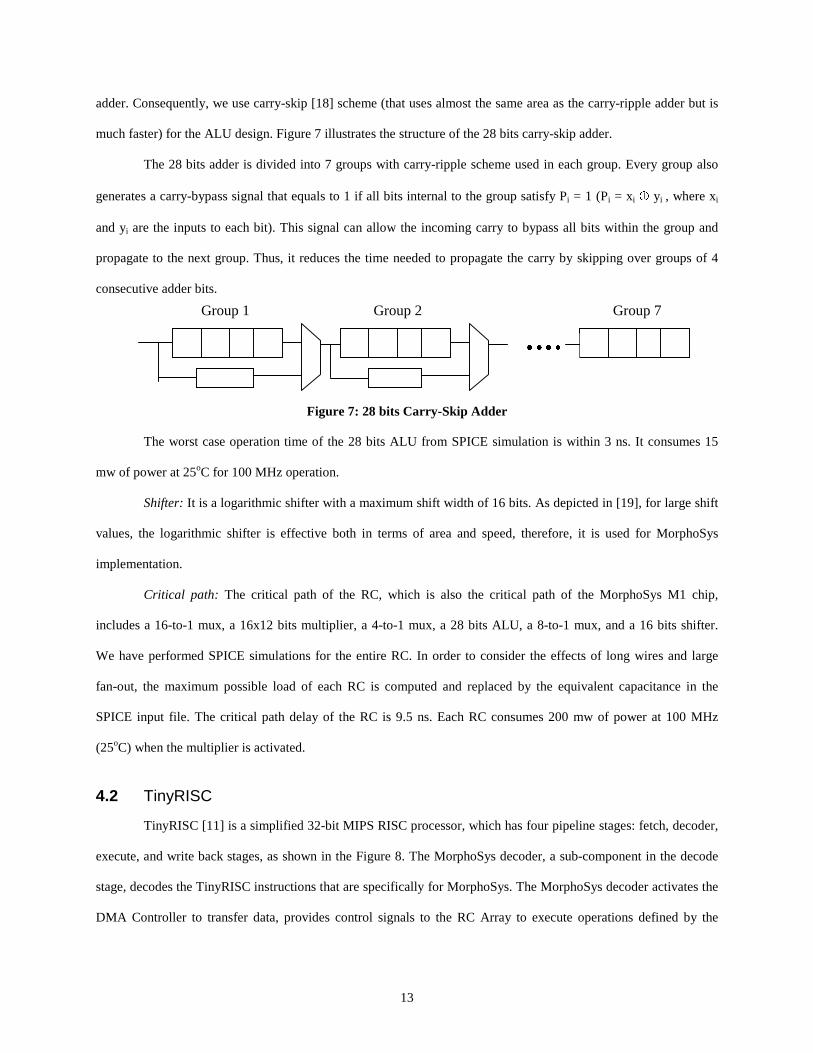
adder. Consequently, we use carry-skip [18] scheme (that uses almost the same area as the carry-ripple adder but is
much faster) for the ALU design. Figure 7 ill ustrates the structure of the 28 bits carry-skip adder.
The 28 bits adder is divided into 7 groups with carry-ripple scheme used in each group. Every group also
generates a carry-bypass signal that equals to 1 if all bits internal to the group satisfy Pi = 1 (Pi = xi � yi , where xi
and yi are the inputs to each bit). This signal can allow the incoming carry to bypass all bits within the group and
propagate to the next group. Thus, it reduces the time needed to propagate the carry by skipping over groups of 4
consecutive adder bits.
Figure 7: 28 bits Carr y-Skip Adder
The worst case operation time of the 28 bits ALU from SPICE simulation is within 3 ns. It consumes 15
mw of power at 25oC for 100 MHz operation.
Shifter: It is a logarithmic shifter with a maximum shift width of 16 bits. As depicted in [19], for large shift
values, the logarithmic shifter is effective both in terms of area and speed, therefore, it is used for MorphoSys
implementation.
Critical path: The critical path of the RC, which is also the critical path of the MorphoSys M1 chip,
includes a 16-to-1 mux, a 16x12 bits multiplier, a 4-to-1 mux, a 28 bits ALU, a 8-to-1 mux, and a 16 bits shifter.
We have performed SPICE simulations for the entire RC. In order to consider the effects of long wires and large
fan-out, the maximum possible load of each RC is computed and replaced by the equivalent capacitance in the
SPICE input file. The critical path delay of the RC is 9.5 ns. Each RC consumes 200 mw of power at 100 MHz
(25oC) when the multiplier is activated.
4.2 TinyRISC
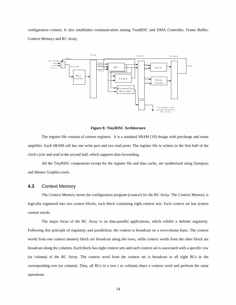
TinyRISC [11] is a simplified 32-bit MIPS RISC processor, which has four pipeline stages: fetch, decoder,
execute, and write back stages, as shown in the Figure 8. The MorphoSys decoder, a sub-component in the decode
stage, decodes the TinyRISC instructions that are specifically for MorphoSys. The MorphoSys decoder activates the
DMA Controller to transfer data, provides control signals to the RC Array to execute operations defined by the
� � � �
Group 1 Group 2 Group 7
14
configuration context. It also establishes communication among TinyRISC and DMA Controller, Frame Buffer,
Context Memory and RC Array.
P C + 1
D est
S r c 2
S r c 1
I F / I DE X / W BI D / E X
R F
M o r p h o S y sD e c o d e r
C o m p
T o D M A C , F B ,C o n t ex t M em o r y ,
R C A r r ay
MU
X
Ju m p
N ex t P C A L U
D a t aC a c h e
O P 1
O P 2
A d d r
D at a
I n s tC a c h e
P C + O f f se t
d a t a
Figure 8: TinyRISC Architecture
The register file consists of sixteen registers. It is a standard SRAM [19] design with precharge and sense
amplifier. Each SRAM cell has one write port and two read ports. The register file is written in the first half of the
clock cycle and read in the second half, which supports data forwarding.
All the TinyRISC components except for the register file and data cache, are synthesized using Synopsys
and Mentor Graphics tools.
4.3 Context Memory
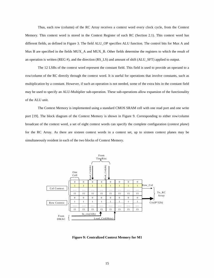
The Context Memory stores the configuration program (context) for the RC Array. The Context Memory is
logically organized into two context blocks, each block containing eight context sets. Each context set has sixteen
context words.
The major focus of the RC Array is on data-parallel applications, which exhibit a definite regularity.
Following this principle of regularity and parallelism, the context is broadcast on a row/column basis. The context
words from one context memory block are broadcast along the rows, while context words from the other block are
broadcast along the columns. Each block has eight context sets and each context set is associated with a specific row
(or column) of the RC Array. The context word from the context set is broadcast to all eight RCs in the
corresponding row (or column). Thus, all RCs in a row ( or column) share a context word and perform the same
operations.
15
Thus, each row (column) of the RC Array receives a context word every clock cycle, from the Context
Memory. This context word is stored in the Context Register of each RC (Section 2.1). This context word has
different fields, as defined in Figure 3. The field ALU_OP specifies ALU function. The control bits for Mux A and
Mux B are specified in the fields MUX_A and MUX_B. Other fields determine the registers to which the result of
an operation is written (REG #), and the direction (RS_LS) and amount of shift (ALU_SFT) applied to output.
The 12 LSBs of the context word represent the constant field. This field is used to provide an operand to a
row/column of the RC directly through the context word. It is useful for operations that involve constants, such as
multiplication by a constant. However, if such an operation is not needed, some of the extra bits in the constant field
may be used to specify an ALU-Multiplier sub-operation. These sub-operations allow expansion of the functionali ty
of the ALU unit.
The Context Memory is implemented using a standard CMOS SRAM cell with one read port and one write
port [19]. The block diagram of the Context Memory is shown in Figure 9. Corresponding to either row/column
broadcast of the context word, a set of eight context words can specify the complete configuration (context plane)
for the RC Array. As there are sixteen context words in a context set, up to sixteen context planes may be
simultaneously resident in each of the two blocks of Context Memory.
0
1
….
15
0
1
….
15
0
1
….
15
0
1
….
15
0
1
….
15
0
1
….
15
0
1
….
15
0
1
….
15
0
1
….
15
0
1
….
15
0
1
….
15
0
1
….
15
0
1
….
15
0
1
….
15
0
1
….
15
0
1
….
15
Col Context
Row Context
In_ctx(32b)
Load_Ctrl(9bits)From
DM AC
Re
ad_C
trl(
6b)
Mas
k_C
trl(
4b)
FromTinyRisc
Ctx(8*32b)
Row_Col
To_RCArray
OneCell
Figure 9: Centralized Context Memory for M1
16
Dynamic reconfiguration: When the Context Memory needs to be changed in order to perform some
different part of an application, the context update can be performed concurrently with RC Array execution. This
dynamic reconfiguration enables the reduction of effective reconfiguration time to zero.
Selective Context Enabling: This implies that only one specific row or column may be enabled for
operation in the RC Array. This feature is primarily useful in loading data into the RC Array. Since context can be
used selectively, and because data bus design allows loading of one column at a time, one set of context words can
be used repeatedly to load data into all eight columns of the RC Array. Without this feature, eight context planes
(out of 32 available) would be required just to read/write data. This feature also allows irregular operations in RC
Array, for e.g. zigzag re-arrangement of array elements.
4.4 Frame Buffer
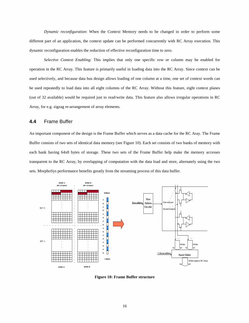
An important component of the design is the Frame Buffer which serves as a data cache for the RC Aray. The Frame
Buffer consists of two sets of identical data memory (see Figure 10). Each set consists of two banks of memory with
each bank having 64x8 bytes of storage. These two sets of the Frame Buffer help make the memory accesses
transparent to the RC Array, by overlapping of computation with the data load and store, alternately using the two
sets. MorphoSys performance benefits greatly from the streaming process of this data buffer.
……. …...
64 bits 64 bits
Barrel ShifterColumn address
64 bits output to RC Array
RowAddressDecoder
First read port
Second read port
Row address
BANK A
(64 x 8 bytes)
BANK A BANK B
SET 0
SET 1
MSByte
LSByte
AA
AA
AA
AA
AA
AA
AA
AA
BB
BB
BB
BB
BB
BB
BB
BB
BANK B
(64 x 8 bytes)
Figure 10: Frame Buffer structure
17
� � � � � � � � � �M
UX
MU
X
RO
WD
EC
OD
ER
64x64 SRAMBANK A
MU
X
RO
WD
EC
OD
ER
64x64 SRAMBANK B
RO
WD
EC
OD
ER
64x64 SRAMBANK A
RO
WD
EC
OD
ER
64x64 SRAMBANK B
MU
X
MU
XM
UX
MU
X
3-STATE
3-ST
AT
E3-
STA
TE
3-ST
AT
E3-
STA
TE
3-STATE
COLUM NOFFSET
COLUM NOFFSET
COLUM NOFFSET
COLUM NOFFSET
DMA_1_WE
DMA_1_WE
bidir � � �� � � � � �
� � � � �
� � � � �
� ! "#$
% & ' ( ) *+ , - .
% & ' ( ) *+ , - .
/ 0 ( ) * � �
/ 0 ( ) * � %
� � � � %
� � � � %
/ 0 ( ) * � �
/ 0 ( ) * � %
% & ' ( ) *+ , - .
% & ' ( ) *+ , - .
1 2 � � � � � �
3 4 � % � � �
56 "7 "#$
� 8 / 9 : � ;( ) . ) +
� 8 / 9 : � ;
< = � �> ? @ � � � �
A B > � C � � � � � �
A B � � C � � � � � �
D E D F G H F I J J K L M N O PK Q F R E S F K E I J
K Q F R E S F R E T E Q SD E D F G H F U K V S E
D E D F G H F H I W X F R E T E Q S
YZ [Z\]^\ [\__`a b cde
fg hgijki hlmn hmffopqrs tuv
YZ [Z\]^ [wxyxz{
YZ [|`
YZ [`_
YZ [Z\]^Z [\__`a b cde
fg hgijkg hlmn hmffopqrs tuv
A B �A B >
� �
� � � �
� �
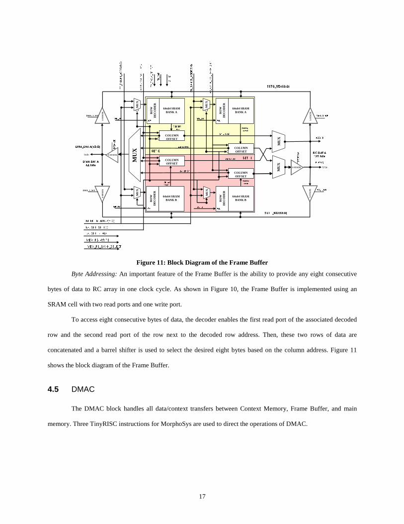
Figure 11: Block Diagram of the Frame Buffer
Byte Addressing: An important feature of the Frame Buffer is the abil ity to provide any eight consecutive
bytes of data to RC array in one clock cycle. As shown in Figure 10, the Frame Buffer is implemented using an
SRAM cell with two read ports and one write port.
To access eight consecutive bytes of data, the decoder enables the first read port of the associated decoded
row and the second read port of the row next to the decoded row address. Then, these two rows of data are
concatenated and a barrel shifter is used to select the desired eight bytes based on the column address. Figure 11
shows the block diagram of the Frame Buffer.
4.5 DMAC
The DMAC block handles all data/context transfers between Context Memory, Frame Buffer, and main
memory. Three TinyRISC instructions for MorphoSys are used to direct the operations of DMAC.
18
Inp
ut L
atch
es -
In
stru
ctio
n H
old
16
16
4
DM A _TR_A ck
Set_Select
FB_B ank_Sel
RC_FB_Select
L oad_Store
DM A _Enable
L d_Row _Col
TR_D ata_Byte_Num
TR_D M A _M em_A ddr
DA T A REG I ST ER
UNI T(DRU )
ST A TE M AC H I NE
AD D RESS G EN ERA T O R
UN I T(A G U)
Glb_Reset
Sys_Clk
64DM A _FB_Data
DM A _M em_Data
16M em_A ddr
8
8DM A _Ctx_A ddr
DM A _FB_A ddrL d_Context_Num
L d_Row _Col_N um
16
32
32
DM A _Ctx_D ata
3
DM A _FB_Rd
DM A _FB_W r
M em_ReadM em_W ri te
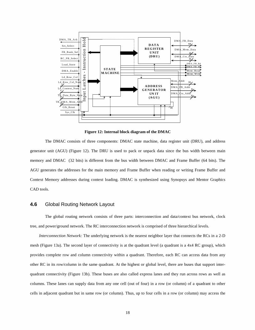
Figure 12: Internal block diagram of the DMAC
The DMAC consists of three components: DMAC state machine, data register unit (DRU), and address
generator unit (AGU) (Figure 12). The DRU is used to pack or unpack data since the bus width between main
memory and DMAC (32 bits) is different from the bus width between DMAC and Frame Buffer (64 bits). The
AGU generates the addresses for the main memory and Frame Buffer when reading or writing Frame Buffer and
Context Memory addresses during context loading. DMAC is synthesized using Synopsys and Mentor Graphics
CAD tools.
4.6 Global Routing Network Layout
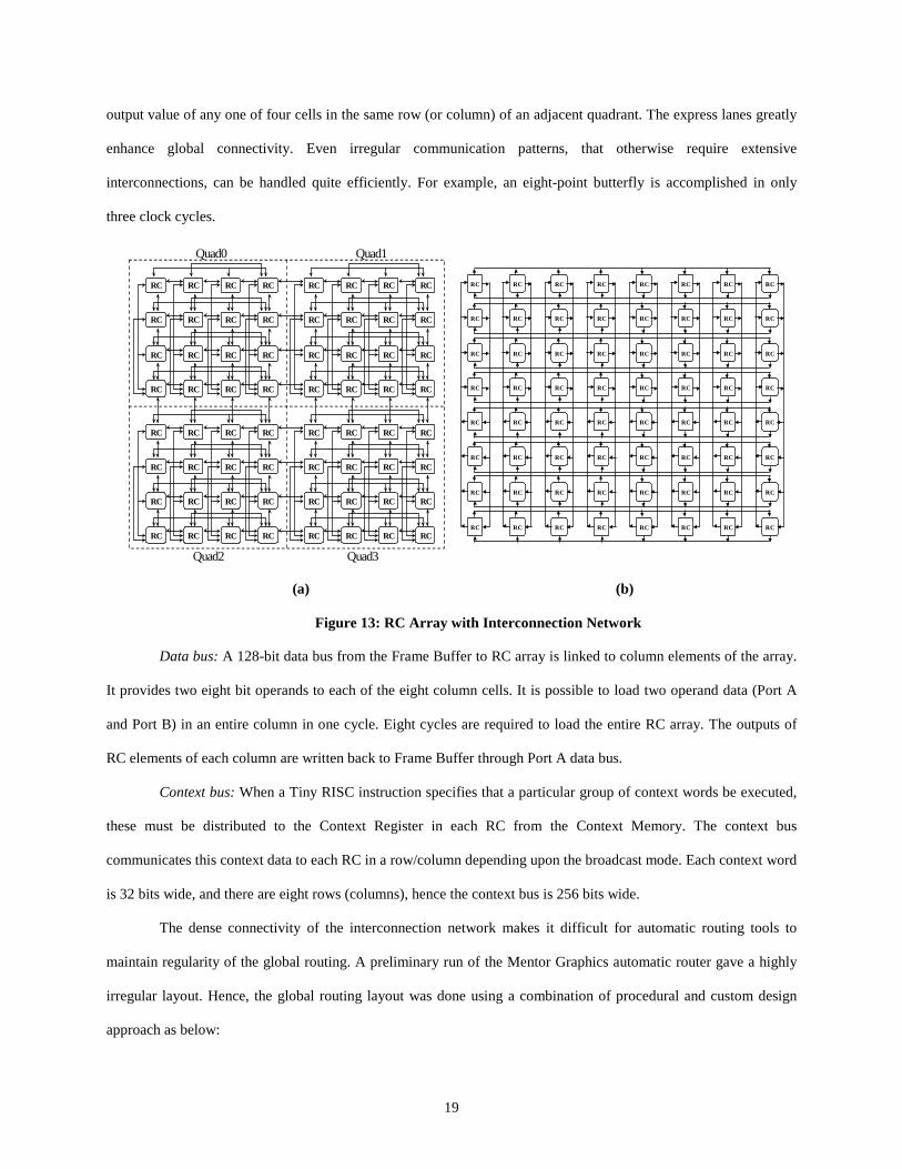
The global routing network consists of three parts: interconnection and data/context bus network, clock
tree, and power/ground network. The RC interconnection network is comprised of three hierarchical levels.
Interconnection Network: The underlying network is the nearest neighbor layer that connects the RCs in a 2-D
mesh (Figure 13a). The second layer of connectivity is at the quadrant level (a quadrant is a 4x4 RC group), which
provides complete row and column connectivity within a quadrant. Therefore, each RC can access data from any
other RC in its row/column in the same quadrant. At the highest or global level, there are buses that support inter-
quadrant connectivity (Figure 13b). These buses are also called express lanes and they run across rows as well as
columns. These lanes can supply data from any one cell (out of four) in a row (or column) of a quadrant to other
cells in adjacent quadrant but in same row (or column). Thus, up to four cells in a row (or column) may access the
19
output value of any one of four cells in the same row (or column) of an adjacent quadrant. The express lanes greatly
enhance global connectivity. Even irregular communication patterns, that otherwise require extensive
interconnections, can be handled quite efficiently. For example, an eight-point butterfly is accomplished in only
three clock cycles.
RC
RC
RC
RC
RC
RC
RC
RC
RC
RC
RC
RC
RC
RC
RC
RC
RC
RC
RC
RC
RC
RC
RC
RC
RC
RC
RC
RC
RC
RC
RC
RC
RC
RC
RC
RC
RC
RC
RC
RC
RC
RC
RC
RC
RC
RC
RC
RC
RC
RC
RC
RC
RC
RC
RC
RC
RC
RC
RC
RC
RC
RC
RC
RC
RC RC
RC RC
RC RC
RC RC
RC RC
RC RC
RC RC
RC RC
RC RC
RC RC
RC RC
RC RC
RC RC
RC RC
RC RC
RC RC
RC RC
RC RC
RC RC
RC RC
RC RC
RC RC
RC RC
RC RC
RC RC
RC RC
RC RC
RC RC
RC RC
RC RC
RC RC
RC RC
Quad0 Quad1
Quad2 Quad3
(a) (b)
Figure 13: RC Arr ay with Interconnection Network
Data bus: A 128-bit data bus from the Frame Buffer to RC array is linked to column elements of the array.
It provides two eight bit operands to each of the eight column cells. It is possible to load two operand data (Port A
and Port B) in an entire column in one cycle. Eight cycles are required to load the entire RC array. The outputs of
RC elements of each column are written back to Frame Buffer through Port A data bus.
Context bus: When a Tiny RISC instruction specifies that a particular group of context words be executed,
these must be distributed to the Context Register in each RC from the Context Memory. The context bus
communicates this context data to each RC in a row/column depending upon the broadcast mode. Each context word
is 32 bits wide, and there are eight rows (columns), hence the context bus is 256 bits wide.
The dense connectivity of the interconnection network makes it difficult for automatic routing tools to
maintain regularity of the global routing. A preliminary run of the Mentor Graphics automatic router gave a highly
irregular layout. Hence, the global routing layout was done using a combination of procedural and custom design
approach as below:
20
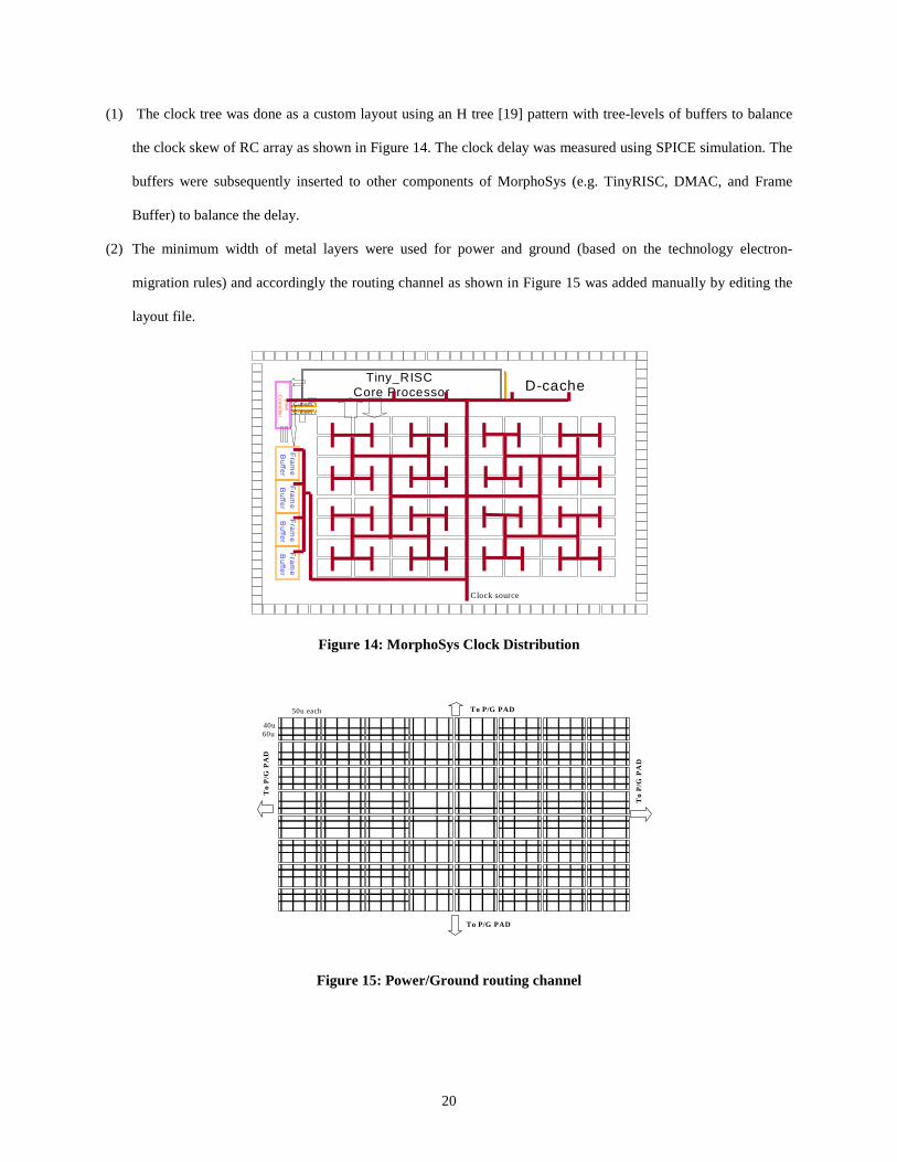
(1) The clock tree was done as a custom layout using an H tree [19] pattern with tree-levels of buffers to balance
the clock skew of RC array as shown in Figure 14. The clock delay was measured using SPICE simulation. The
buffers were subsequently inserted to other components of MorphoSys (e.g. TinyRISC, DMAC, and Frame
Buffer) to balance the delay.
(2) The minimum width of metal layers were used for power and ground (based on the technology electron-
migration rules) and accordingly the routing channel as shown in Figure 15 was added manually by editing the
layout file.
DM
A
Co
ntro
ller
Fra
me
Bu
ffer
Fra
me
Bu
ffer
Fra
me
Bu
ffer
Fra
me
Bu
ffer
C-mem
C-mem
D-cacheTiny_RISC
Core Processor
Clock source
Figure 14: MorphoSys Clock Distr ibution
T o P/G PAD
T o P/G PAD
To
P/G
PA
D
To
P/G
PA
D
50u each
40u60u
Figure 15: Power/Ground routing channel
21
(3) The regular pattern of the interconnection network were captured using function calls that perform the
procedural routing for creating the layout. We partitioned the interconnection network into four types of
connectivity:
(a) intra-quadrant row/column full connectivity.
(b) inter-quadrant context connectivity.
(c) inter-quadrant express lane connectivity.
(d) cross quadrant boundary connectivity.
For (a) and (b), the routing channels are fixed for all RCs. For (c) and (d), the channels switch direction when
crossing the quadrant boundary. Once the pattern of each RC is figured out, the routing of the interconnection
network can be performed easil y.
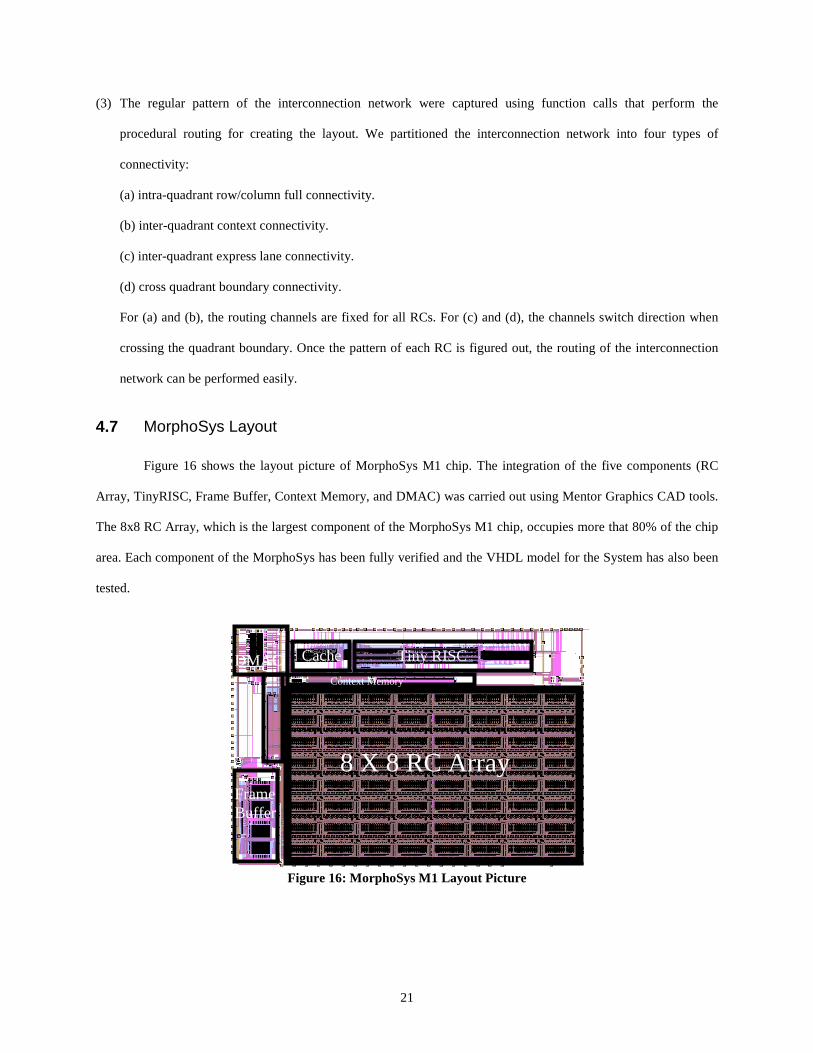
4.7 MorphoSys Layout
Figure 16 shows the layout picture of MorphoSys M1 chip. The integration of the five components (RC
Array, TinyRISC, Frame Buffer, Context Memory, and DMAC) was carried out using Mentor Graphics CAD tools.
The 8x8 RC Array, which is the largest component of the MorphoSys M1 chip, occupies more that 80% of the chip
area. Each component of the MorphoSys has been fully verified and the VHDL model for the System has also been
tested.
Figure 16: MorphoSys M1 Layout Picture
8 X 8 RC Array
Tiny RISCCache
FrameBuffer
DMACContext Memory
22
Table 4 lists the transistor count of each component and Table 5 summarizes the features of the MorphoSys
M1 chip.
Table 4: Transistor Count of MorphoSys M1 chip
Component Transistor Count
RC Array 1,195,392
Frame Buffer 139,106
TinyRISC 92,128
Context Memory 105,096
DMAC 20,594
MorphoSys Decoder 3,910
Main Memory Controller 1,180
Total 1,557,406
Table 5: MorphoSys M1 Chip Features
Process Technology HP CMOS, 0.35 } m ,3.3 V, four-layer-metal
Area 14mm x 12mm
Transistor count 1,557,406
Peak performance 6.4 GOPS on 16 bits data
Clock frequency 100 MHz
Power consumption
( 100 MHz, 25o C )
15W in the worst case< 7W for DCT
< 5W for motion estimationPin count 240 (132 I/O, 54 power, 54 groung)
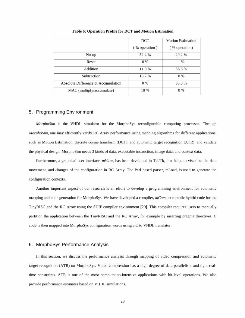
In Table 5, we provide three numbers for the power consumption. In the worst case where the multiplier of
each RC is activated in each clock cycle, the power consumption is 15 W. However, among the applications we
have investigated, there is no such case that the multiplier of each RC is enabled in each clock cycle. In order to get
a more realistic measurement, we also estimated the power consumption for DCT and motion estimation. We use
Hspice to simulate the power consumption of each function shown in Table 2 with the worst case scenario, which
means each bit of the input switches every clock cycle. The power consumption of the MorphoSys is accordingly
estimated based on percentage of each operation in our application mapping context shown in Table 6. The results
show a difference from the worst case by more than a factor of 2.
23
Table 6: Operation Profile for DCT and Motion Estimation
DCT
( % operation )
Motion Estimation
( % operation)
No-op 52.4 % 29.2 %
Reset 0 % 1 %
Addition 11.9 % 36.5 %
Subtraction 16.7 % 0 %
Absolute Difference & Accumulation 0 % 33.3 %
MAC (multiply/accumulate) 19 % 0 %
5. Programming Environment
MorphoSim is the VHDL simulator for the MorphoSys reconfigurable computing processor. Through
MorphoSim, one may efficiently verify RC Array performance using mapping algorithms for different applications,
such as Motion Estimation, discrete cosine transform (DCT), and automatic target recognition (ATR), and validate
the physical design. MorphoSim needs 3 kinds of data: executable instruction, image data, and context data.
Furthermore, a graphical user interface, mView, has been developed in Tcl/Tk, that helps to visualize the data
movement, and changes of the configuration in RC Array. The Perl based parser, mLoad, is used to generate the
configuration contexts.
Another important aspect of our research is an effort to develop a programming environment for automatic
mapping and code generation for MorphoSys. We have developed a compiler, mCom, to compile hybrid code for the
TinyRISC and the RC Array using the SUIF compiler environment [20]. This compiler requires users to manually
partition the application between the TinyRISC and the RC Array, for example by inserting pragma directives. C
code is then mapped into MorphoSys configuration words using a C to VHDL translator.
6. MorphoSys Performance Analysis
In this section, we discuss the performance analysis through mapping of video compression and automatic
target recognition (ATR) on MorphoSys. Video compression has a high degree of data-parallelism and tight real-
time constraints. ATR is one of the most computation-intensive applications with bit-level operations. We also
provide performance estimates based on VHDL simulations.
24
6.1 Video Compression: Motion Estimation for MPEG
Motion Estimation is the most computation-intensive algorithm in MPEG. Among the different algorithms,
full search block matching (FSBM) [21] involves the maximum computations, however, gives an optimal solution
with low control overhead. The detail description of the mapping can be found in [12]. For a reference block size of
16x16 and image size of 352x288 pixels at 30 frames per second (MPEG-2 main profile, low level), the processing
of an entire image takes about 21.0 ms on a 100 MHz MorphoSys. This is much faster than the frame period of
33.33ms.
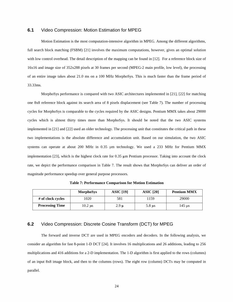
MorphoSys performance is compared with two ASIC architectures implemented in [21], [22] for matching
one 8x8 reference block against its search area of 8 pixels displacement (see Table 7). The number of processing
cycles for MorphoSys is comparable to the cycles required by the ASIC designs. Pentium MMX takes about 29000
cycles which is almost thirty times more than MorphoSys. It should be noted that the two ASIC systems
implemented in [21] and [22] used an older technology. The processing unit that constitutes the critical path in these
two implementations is the absolute difference and accumulation unit. Based on our simulation, the two ASIC
systems can operate at about 200 MHz in 0.35 ~ m technology. We used a 233 MHz for Pentium MMX
implementation [23], which is the highest clock rate for 0.35 ~ m Pentium processor. Taking into account the clock
rate, we depict the performance comparison in Table 7. The result shows that MorphoSys can deliver an order of
magnitude performance speedup over general purpose processors.
Table 7: Performance Compar ison for Motion Estimation
MorphoSys ASIC [19] ASIC [20] Pentium MMX
# of clock cycles 1020 581 1159 29000
Processing Time 10.2 ~ s 2.9 ~ 5.8 ~ s 145 ~ s
6.2 Video Compression: Discrete Cosine Transform (DCT) for MPEG
The forward and inverse DCT are used in MPEG encoders and decoders. In the following analysis, we
consider an algorithm for fast 8-point 1-D DCT [24]. It involves 16 multiplications and 26 additions, leading to 256
multiplications and 416 additions for a 2-D implementation. The 1-D algorithm is first applied to the rows (columns)
of an input 8x8 image block, and then to the columns (rows). The eight row (column) DCTs may be computed in
parallel.

25
The cost for computing 2-D DCT on an 8x8 block of the image is as follows: 6 cycles for butterfly, 12
cycles for both 1-D DCT computations and 3 cycles are used for re-arrangement and scaling of data (giving a total
of 21 cycles). This estimate is verified by VHDL simulation. Assuming the data blocks to be present in the RC
Array (through overlapping of data load/store with computation cycles), it would take 0.49 ms for MorphoSys to
compute the DCT for all 8x8 blocks (396x6) in one frame of a 352x288 image. The cost of computing the 2-D IDCT
is the same, because the steps involved are similar. Context loading time is quite significant at 270 cycles. However,
this effect is minimized through transforming a large number of blocks (typically 2376 blocks) before a different
configuration is loaded.
MorphoSys requires 21 cycles to complete 2-D DCT (or IDCT) on 8x8 block of pixel data. This is in
contrast to 240 cycles required by Pentium MMX TM [23]. Even a dedicated superscalar multi-media processor [25]
requires 201 clocks for the IDCT. REMARC [9] takes 54 cycles to implement the IDCT, even though it uses 64
nano-processors. For the comparison of processing time, we use the clock rate of 200 MHz V830R/AV as presented
in [25] although V830R/AV is implemented using 0.25 � m technology. REMARC has similar processing power (in
terms of processing elements) to MorphoSys, so we assume 100 MHz for REMARC. The comparison is
summarized is Table 8.
Table 8: Performance Compar ison for DCT/IDCT
MorphoSys REMARC V830R/AV Pentium MMX
# of clock cycles 21 54 201 240
Processing time 210 ns 540 ns 1005 ns 1200 ns
6.3 Automatic Target Recognition (ATR)
Automatic Target Recognition (ATR) is the machine function of detecting, classifying, recognizing, and
identifying an object without human intervention. The ATR processing model [26] developed at Sandia National
Laboratory has been mapped to MorphoSys [12].
For performance analysis, we chose the system parameters that were used in [26]. The ATR systems
implemented in [26] and [27] were used for comparison. Two Xil inx 4013 FPGAs (one dynamic FPGA for most of
the computations and one static FPGA for control) are used in Mojave [26], and Splash 2 system (consisting of 16
Xili nx 4010 chips) is discussed in [27]. For this study, the image size is 128x128 pixels, and the size of the target
26
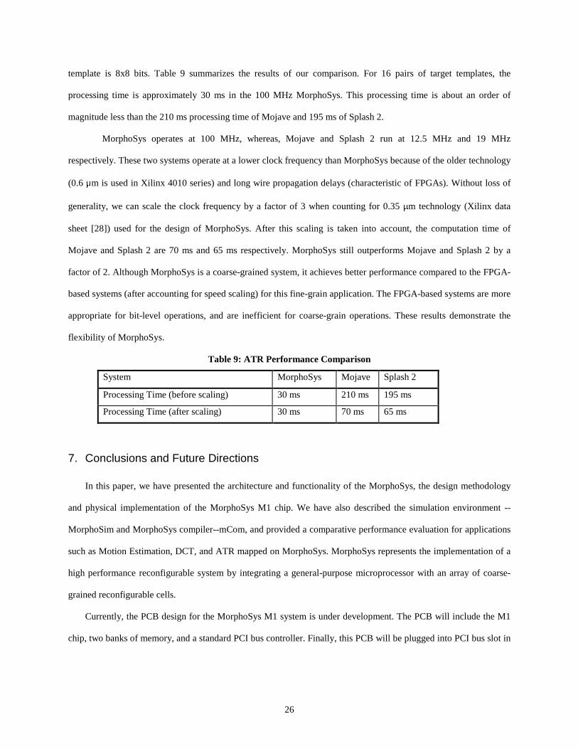
template is 8x8 bits. Table 9 summarizes the results of our comparison. For 16 pairs of target templates, the
processing time is approximately 30 ms in the 100 MHz MorphoSys. This processing time is about an order of
magnitude less than the 210 ms processing time of Mojave and 195 ms of Splash 2.
MorphoSys operates at 100 MHz, whereas, Mojave and Splash 2 run at 12.5 MHz and 19 MHz
respectively. These two systems operate at a lower clock frequency than MorphoSys because of the older technology
(0.6 � m is used in Xilinx 4010 series) and long wire propagation delays (characteristic of FPGAs). Without loss of
generality, we can scale the clock frequency by a factor of 3 when counting for 0.35 � m technology (Xil inx data
sheet [28]) used for the design of MorphoSys. After this scaling is taken into account, the computation time of
Mojave and Splash 2 are 70 ms and 65 ms respectively. MorphoSys still outperforms Mojave and Splash 2 by a
factor of 2. Although MorphoSys is a coarse-grained system, it achieves better performance compared to the FPGA-
based systems (after accounting for speed scaling) for this fine-grain application. The FPGA-based systems are more
appropriate for bit-level operations, and are inefficient for coarse-grain operations. These results demonstrate the
flexibili ty of MorphoSys.
Table 9: ATR Performance Compar ison
System MorphoSys Mojave Splash 2
Processing Time (before scaling) 30 ms 210 ms 195 ms
Processing Time (after scaling) 30 ms 70 ms 65 ms
7. Conclusions and Future Directions
In this paper, we have presented the architecture and functionality of the MorphoSys, the design methodology
and physical implementation of the MorphoSys M1 chip. We have also described the simulation environment --
MorphoSim and MorphoSys compiler--mCom, and provided a comparative performance evaluation for applications
such as Motion Estimation, DCT, and ATR mapped on MorphoSys. MorphoSys represents the implementation of a
high performance reconfigurable system by integrating a general-purpose microprocessor with an array of coarse-
grained reconfigurable cells.
Currently, the PCB design for the MorphoSys M1 system is under development. The PCB will include the M1
chip, two banks of memory, and a standard PCI bus controller. Finally, this PCB will be plugged into PCI bus slot in
27
the host PC to do the final test and the real performance evaluation. Meanwhile, we are continuing to develop the
current compiler to provide the automatic partitioning of applications into sequential and data-parallel parts.
8. Acknowledgments
This research is funded by the Defense and Advanced Research Projects Agency (DARPA) of the Department
of Defense under the contract number F-33615-97-C-1126.
References:
1. W.H.Mangione-Smith, B.Hutchings, D.Andrews, A.DeHon, C.Ebeling, R.Hartenstein, O.Mencer, J.Morris,
K.Palem, V.K.Prasanna, H.A.E.Spaaneburg, “Seeking Solutions in Configurable Computing,” IEEE Computer,
Dec 1997, pp. 38-43.
2. S. Brown and J. Rose, “Architecture of FPGAs and CPLDs: A Tutorial,” IEEE Design and Test of Computers,
Vol. 13, No. 2, pp. 42-57, 1996.
3. M. Gokhale, W. Holmes, A. Kopser, S. Lucas, R. Minnich, D. Sweely, D. Lopresti, “Building and Using a
Highly Parallel Programmable Logic Array,” IEEE Computer, pp. 81-89, Jan. 1991
4. E. Tau, D. Chen, I. Eslick, J. Brown and A. DeHon, “A First Generation DPGA Implementation,” FPD’95,
Canadian Workshop of Field-Programmable Devices, May 1995.
5. J. R. Hauser and J. Wawrzynek, “Garp: A MIPS Processor with a Reconfigurable Co-processor,” Proc. of the
IEEE Symposium on FPGAs for Custom Computing Machines, 1997.
6. D.C.Chen, J.M.Rabaey, “A Reconfigurable Multi-processor IC for Rapid Prototyping of Algorithmic-Specific
HighSpeed Datapaths,” IEEE Journal of Solid-State Circuits,V.27, No.12, Dec 1992.
7. E. Mirsky and A. DeHon, “MATRIX: A Reconfigurable Computing Architecture with Configurable Instruction
Distribution and Deployable Resources,” IEEE Symposium on FCCM, 1996, pp.157-66.
8. C. Ebeling, D. Cronquist, and P. Franklin "Configure Computing: The Catalyst for High-performance
Architectures", Proeedings of IEEE International Conference on Application-specific Systems, Architectures
and Processors, July 1997, pp. 364-72.
28
9. T. Miyamori and K. Olukotun, “A Quantitative Analysis of Reconfigurable Coprocessors for Multimedia
Applications” , Proceedings of IEEE Symposium on Field-Programmable Custom Computing Machines, April
1998.
10. J. Babb, M. Frank, V. Lee, E. Waingold, R. Barua, M. Taylor, J. Kim, S. Devabhaktuni, A. Agrawal, “The
RAW Benchmark Suite: computation structures for general-purpose computing,” Proc. IEEE Symposium on
Field-Programmable Custom Computing Machines, FCCM 97, 1997, pp. 134-43
11. A.Abnous, C.Christensen,J.Gray,J.Lenell,A.Naylor and N.Bagherzaheh, “Design and implementation of
TinyRISC microprocessor” Microprocessors and Microsystems, Vol.16, No.4, pp.187-94, 1992.
12. H. Singh, M. Lee, G. Lu, F. Kurdahi, N. Bagherzadeh, T. Lang, R. Heaton, E. Filho, "Morphosys: An Integrated
Re-configurable Architecture"NATO Symposium on Concepts and Integration, April , 1998.
13. K.Yano, T. Yamanaka, T. Nishida, M. Saito, K. Shimohigashi, and A. Shimizu, "A 3.8-ns CMOS 16 x 16-b
Multiplier Using Complementary Pass-Transistor Logic", IEEE Jurnal of Solid-State Circuits, vol 25, no. 2, pp.
388-395, April 1990.
14. T. K. Callaway and E. E. Swartzlander, Jr. "The Power Consumption of CMOS Adders and Multipliers", Low
Power CMOS Design, IEEE Press, 1998, edited by A.Chandrakasan, R. Brodersen.
15. C. S. Wallace, "A Suggestion for a Fast Multiplier", IEEE Transactions on Electronic Computer, vol.EC-13,
pp.14-17, 1964.
16. L. Dadda, "Some Schemes for Parallel Multipliers", Alta Freq., vol.34, pp.349-356, 1965
17. C.R Baugh and B.A. Wooly, "A Two's Complement Parallel Array Multiplication Algorithm", IEEE
Transactions on Computer, C-22(12):1045-1047, Dec 1973.
18. I. Koren, Computer Arithmetic Algorithms, Prentice Hall Inc, 1993.
19. J. M. Rabaey, Digital Integrated Circuits A Design Perspective. Prentice Hall Inc, 1996.
20. SUIF Compiler system, The Stanford SUIF Compiler Group, http://suif.stanford.edu.
21. C. Hsieh, T. Lin, “VLSI Architecture For Block-Matching Motion Estimation Algorithm,” IEEE Trans. on
Circuits and Systems for Video Tech., vol. 2, pp. 169-175, June 1992.
22. K-M Yang, M-T Sun and L. Wu, “ A Family of VLSI Designs for Motion Compensation Block Matching
Algorithm,” IEEE Trans. on Circuits and Systems, V. 36, No. 10, Oct 89, pp. 1317-25.
23. Intel Application Notes for Pentium MMX, http://developer.intel.com/drg/mmx/appnotes/
29
24. W-H Chen, C. H. Smith and S. C. Fralick, “A Fast Computational Algorithm for the Discrete Cosine
Transform,” IEEE Trans. on Comm., vol. COM-25, No. 9, September 1977.
25. T. Arai, I. Kuroda, K. Nadehara and K. Suzuki, “V830R/AV: Embedded Multimedia Superscalar RISC
Processor,” IEEE MICRO, Mar/Apr 1998, pp. 36-47.
26. J. Vill asenor, B. Schoner, K. Chia, C. Zapata, H. J. Kim, C. Jones, S. Lansing, and B. Mangione-Smith, “
Configurable Computing Solutions for Automatic Target Recognition,” Proceedings of IEEE Workshop on
FPGAs for Custom Computing Machine, April 1996.
27. M. Rencher and B.L. Hutchings, " Automated Target Recognition on SPLASH 2 " Proceedings of IEEE
Symposium on FPGAs for Custom Computing Machine, April 1997.
28. XC 4000 Series High-Density Strategy, http://www.xil inx.xom.